Maxq family user’s guide – Maxim Integrated MAXQ Family User Manual
Page 8

2-3
MAXQ Family User’s Guide
SECTION 2: ARCHITECTURE
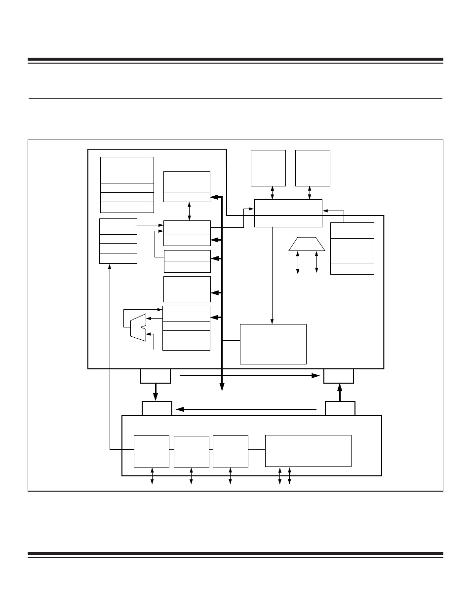
The MAXQ architecture is designed to be modular and expandable. Top-level instruction decoding is extremely simple and based on
transfers to and from registers. The registers are organized into functional modules, which are in turn divided into the System Register
and Peripheral Register groups. Figure 2-1 illustrates the modular architecture and the basic transport possibilities.
SYSTEM MODULES/
REGISTERS
PERIPHERAL MODULES/REGISTERS
DATA
MEMORY
dst
MAXQ PRODUCT SPECIFIC
MODULES
(MULTIPLY ACCUMULATE UNIT,
ADC, DAC, PWM, ETC.)
STACK
MEMORY
CKCN
WDCN
IC
ADDRESS
GENERATION
IP
SP
IC
LOOP COUNTERS
LC[
η]
IIR
IMR
INTERRUPT
LOGIC
CLOCK CONTROL,
WATCHDOG TIMER
AND POWER MONITOR
BOOLEAN
VARIABLE
MANIPULATION
ACCUMULATORS
(16)
AP
APC
PSF
INSTRUCTION
DECODE
(SRC, DST TRANSPORT
DETERMINATION)
MUX
DATA POINTERS
DP[0], DP[1]
FP =
(BP + OFFS)
DPC
SC
MEMORY MANAGEMENT
UNIT (MMU)
PROGRAM
MEMORY
src
dst
src
GENERAL-
PURPOSE
I/O
TIMERS/
COUNTERS
UART
AND SPI
Figure 2-1. MAXQ Transport-Triggered Architecture
Maxim Integrated
- DS80C390 (58 pages)
- DS5001FP (26 pages)
- MAX1416 (14 pages)
- MAX5865 (18 pages)
- DS33Z41 (167 pages)
- MAX1202 (7 pages)
- USBTO232 (31 pages)
- HFAN-09.5.0: Pattern Creator/Converter Software (8 pages)
- MAX-IDE MAXQ Microcontrollers (11 pages)
- MAX6876 Power-Supply Tracker/Sequencer (6 pages)
- MAX6877 Power-Supply Tracker/Sequencer (3 pages)
- 78Q8430 ARM9(920T) Linux Driver Diagnostic Guide (19 pages)
- 78Q8430 Software Driver (54 pages)
- 78Q8430 ST 5100/OS-20 with NexGen TCP/IP Stack (28 pages)
- 6612_OMU_S2_URT_V1_13 (56 pages)
- 6612_OMU_S2+2_URT_V1_14 (58 pages)
- 71M6511 Power Meter IC Family Software (137 pages)
- 71M65xx ADM51 ICE Safety Notice (2 pages)
- 71M6511 2-Layer Demo Board (2 pages)
- 71M6511 4-Layer Demo Board (2 pages)
- 78Q8430 Linux Driver ARM Platform (22 pages)
- 71M6513 Demo Board (2 pages)
- 71M6521DE Energy Meter IC Family Software (138 pages)
- 71M6521 Demo Board (2 pages)
- 71M6531 Demo Board (2 pages)
- 71M6531 Energy Meter IC Family Software (116 pages)
- 71M6533 Demo Board (2 pages)
- 71M6534H Demo Board (2 pages)
- 71M6515H Demo Board (2 pages)
- 73S1209F Evaluation Board (2 pages)
- 73S12xxF (38 pages)
- 73S12xxF Software (93 pages)
- 73S1210F Evaluation Board Lite (2 pages)
- 73S1210F Evaluation Board (2 pages)
- 73S1210F Multi-SAM Evaluation Board Lite (2 pages)
- 73S12xxF USB-CCID Linux DFU Host Application (8 pages)
- 73S1215F Device Firmware Upgrade Host Driver/Application (10 pages)
- 73S12xxF USB-CCID Host GUI (22 pages)
- 73S1215F Windows XP 32 USB CCID and DFU Drivers (15 pages)
- 73S1215F CCID USB Linux Driver (16 pages)
- 73S1215F Evaluation Board (2 pages)
- 73S1215F Evaluation Board Lite (2 pages)
- 73S1217F Evaluation Board (2 pages)
- 73S1217F Evaluation Board Lite (2 pages)
