1 spi transfer formats, 2 spi character lengths, 1 spi transfer formats -3 – Maxim Integrated MAXQ Family User Manual
Page 115: 2 spi character lengths -3, Maxq family user’s guide
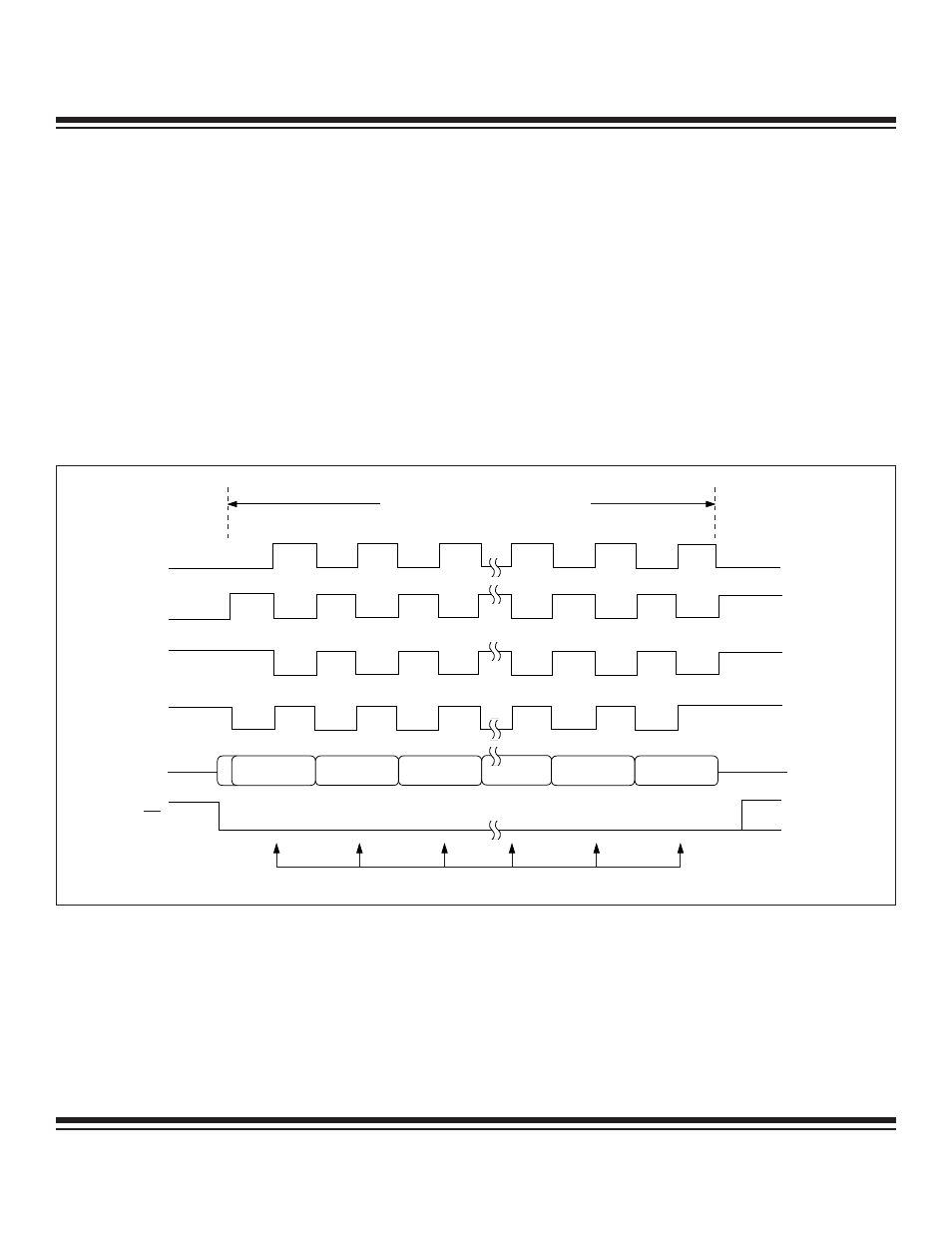
11.1 SPI Transfer Formats
During an SPI transfer, data is simultaneously transmitted and received over two serial data lines with respect to a single serial shift
clock. The polarity and phase of the serial shift clock are the primary components in defining the SPI data transfer format. The polari-
ty of the serial clock corresponds to the idle logic state of the clock line and therefore also defines which clock edge is the active edge.
To define a serial shift clock signal that idles in a logic low state (active clock edge = rising), the Clock Polarity Select (CKPOL; SPICF.0)
bit should be configured to a 0, while setting CKPOL = 1 will cause the shift clock to idle in a logic high state (active clock edge =
falling). The phase of the serial clock selects which edge is used to sample the serial shift data. The Clock Phase Select (CKPHA;
SPICF.1) bit controls whether the active or inactive clock edge is used to latch the data. When CKPHA is set to logic 1, data is sam-
pled on the inactive clock edge (clock returning to the idle state). When CKPHA is set to logic 0, data is sampled on the active clock
edge (clock transition to the active state). Together, the CKPOL and CKPHA bits allow the four possible SPI data transfer formats as
illustrated in Figure 11-2.
Anytime that the active clock edge is used for sampling (CKPHA = 0), the transfer cycle must be started with assertion of the SSEL
signal. This requirement necessitates that the SSEL signal be deasserted and reasserted between successive transfers. Conversely,
when the inactive edge is used for sampling (CKPHA = 1), the SSEL signal may remain low through successive transfers allowing the
active clock edge to signal the start of a new transfer.
11.2 SPI Character Lengths
To flexibly accommodate different SPI transfer data lengths, the character length for any transfer is user configurable through the
Character Length Bit (CHR) in the SPI Configuration Register. The CHR bit allows selection of either 8-bit or 16-bit transfers.
When loading 8-bit characters into the SPIB data buffer, the byte for transmission should be right-justified or placed in the least signif-
icant byte of the word. When a byte transfer completes, the received byte is right-justified and can be read from the least significant
byte of the SPIB word. The MSB of the SPIB data buffer is not significant when transmitting and receiving 8-bit characters.
11-3
MAXQ Family User’s Guide
SPICK
CKPOL = 0
CKPHA = 0
CKPOL = 0
CKPHA = 1
CKPOL = 1
CKPHA = 0
CKPOL = 1
CKPHA = 1
MOSI/MISO
SSEL
SAMPLING POINTS
TRANSFER CYCLE (CHARACTER LENGTH DEFINED BY CHR)
MSBIT
LSBIT
Figure 11-2. SPI Transfer Formats (CKPOL, CKPHA Control)
Maxim Integrated