2 spi configuration reg, 3 spi clock register (s, 2 spi configuration register (spicf) -7 – Maxim Integrated MAXQ Family User Manual
Page 119: 3 spi clock register (spick) -7, Maxq family user’s guide, 2 spi configuration register (spicf), 3 spi clock register (spick)
11-7
MAXQ Family User’s Guide
Bit 0: SPI Enable (SPIEN)
0 = SPI module and its baud-rate generator are disabled
1 = SPI module and its baud-rate generator are enabled
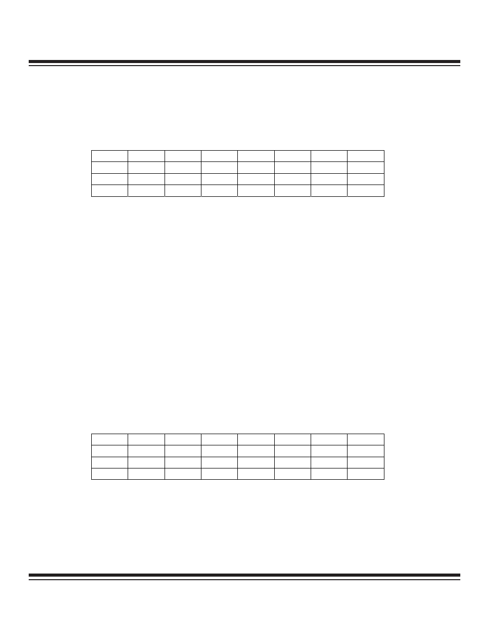
11.7.2 SPI Configuration Register (SPICF)
Bit 7: SPI Interrupt Enable (ESPII). This bit enables any of the SPI interrupt source flags (MODF, WCOL, ROVR, SPIC) to generate
interrupt requests.
0 = SPI interrupt sources disabled
1 = SPI interrupt sources enabled
Bits 6 to 3: Reserved
Bit 2: Character Length Bit (CHR). This bit determines the character length for a SPI transfer cycle. A character can be 8 bits in length
or 16 bits in length.
0 = 8-bit character length specified
1 = 16-bit character length specified
Bit 1: Clock Phase Select (CKPHA). This bit selects the clock phase and is used with the CKPOL bit to define the SPI data transfer
format.
0 = Data sampled on the active clock edge
1 = Data sampled on the inactive clock edge
Bit 0: Clock Polarity Select (CKPOL). This bit selects the clock polarity and is used with the CKPHA bit to define the SPI data trans-
fer format.
0 = Clock idles in the logic 0 state (rising = active clock edge)
1 = Clock idles in the logic 1 state (falling = active clock edge)
11.7.3 SPI Clock Register (SPICK)
Bits 7 to 0: Clock Divider Ratio (CKR.[7:0]). This 8-bit value determines the system clock-divide ratio to be used for SPI master mode
baud-clock generation. This register has no function when operating in slave mode as the SPI clock generation circuitry is disabled.
The frequency of the SPI master mode baud rate is calculated using the following equation:
SPI Baud Rate = (0.5 x System Clock Frequency) / (CKR[7:0] + 1)
Bit #
7
6
5
4
3
2
1
0
Name
ESPII
—
—
—
—
CHR
CKPHA
CKPOL
Reset
0
0
0
0
0
0
0
0
Access
rw
r
r
r
r
rw
rw
rw
r = read, w = write
Bit #
7
6
5
4
3
2
1
0
Name
CKR.7
CKR.6
CKR.5
CKR.4
CKR.3
CKR.2
CKR.1
CKR.0
Reset
0
0
0
0
0
0
0
0
Access
rw
rw
rw
rw
rw
rw
rw
rw
r = read, w = write
Maxim Integrated