4 dr-scan sequence, 4 dr-scan sequence -4, Maxq family user’s guide – Maxim Integrated MAXQ Family User Manual
Page 155
When the parallel instruction register (IR2:0) is updated, the TAP controller decodes the instruction and performs any necessary oper-
ations, including activation of the data shift register to be used for the particular instruction during data register shift sequences (DR-
Scan). The length of the activated shift register depends upon the value loaded to the instruction register (IR2:0). The supported
instruction-register encodings and associated data-register selections are shown in Table 15-2.
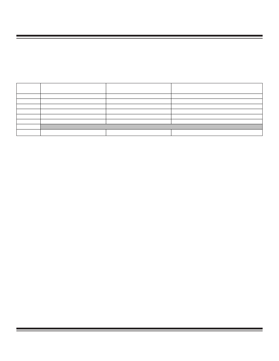
Table 15-2. Instruction Register (IR2:0) Encodings
The Extest (IR2:0 = 000b) and Sample/Preload (IR2:0 = 001b) instructions are mandated by the JTAG standard, however, the MAXQ
microcontroller does not intend to make practical use of these instructions. Hence, these instructions are treated as no operations but
may be entered into the instruction register without affecting the on-chip system logic or pins and does not change the existing serial
data register selection between TDI and TDO.
The By-pass (IR2:0 = 011b, 101b, or 111b) instruction is also mandated by the JTAG standard. The By-pass instruction is fully implemented
by the MAXQ microcontroller to provide a minimum length serial data path between the TDI and the TDO pins. This is accomplished by
providing a single cell bypass shift register. When the instruction register is updated with the By-pass instruction, a single bypass register
bit is connected serially between TDI and TDO in the Shift-DR state. The instruction register automatically defaults to the By-pass instruc-
tion when the TAP is in the Test-Logic-Reset state. The By-pass instruction has no effect on the operation of the on-chip system logic.
The Debug (IR2:0 = 010b) and System Programming (IR2:0 = 100b) instructions are private instructions that are intended solely for in-
circuit debug and in-system programming operations respectively. If the instruction register is updated with the Debug instruction, a 10-
bit serial shift register is formed between the TDI and TDO pins in the Shift-DR state. If the System Programming instruction is entered
into the instruction register (IR2:0), a 3-bit serial data shift register is formed between the TDI and TDO pins in the Shift-DR state.
Instruction register (IR2:0) settings other than those listed and described above are reserved for internal use. As can be seen in
Figure 15-2, the instruction register serves to select the length of the serial data register between TDI and TDO during the Shift-DR
state.
15.2.4 DR-Scan Sequence
Once the instruction register has been configured to a desired state (mode), transactions are performed via a data buffer register asso-
ciated with that mode. These data transactions are executed serially in a manner analogous to the process used to load the instruc-
tion register and are grouped in the TAP Controller state sequence starting from the Select-DR-Scan state. In the TAP controller state
sequence, the Shift-DR state allows internal data to be shifted out through the TDO pin while the external data is shifted in simultane-
ously via the TDI pin. Once a complete data pattern is shifted in, input data can be latched into the parallel buffer of the selected reg-
ister on the falling edge of TCK in the Update-DR state. On the same TCK falling edge, in the Update-DR state, the internal parallel
buffer is loaded to the data shift register for output. This Shift-DR/Update-DR process serves as the basis for passing information
between the external host and the MAXQ microcontroller. These data register transactions occur in the data register portion of the TAP
controller state sequence diagram and have no effect on the instruction register.
15-4
MAXQ Family User’s Guide
IR2:0
INSTRUCTION
FUNCTION
SERIAL DATA SHIFT
REGISTER SELECTION
000
Extest
No operation
Unchanged (retain previous selection)
001
Sample/Preload
No operation
Unchanged (retain previous selection)
010
Debug
In-circuit debug mode
10-bit shift register
011
By-pass
No operation (default)
1-bit shift register
100
System Programming
Bootstrap function
3-bit shift register
101
By-pass
No operation (default)
1-bit shift register
110
Reserved
111
By-pass
No operation (default)
1-bit shift register
Maxim Integrated