2 1-wire clock control, 1 1-wire clock divisor, 2 1-wire clock control -4 – Maxim Integrated MAXQ Family User Manual
Page 133: 1 1-wire clock divisor register (owa = 100b) -4, Maxq family user’s guide

13.2 1-Wire Clock Control
All 1-Wire timing patterns are generated using a base clock of 1.0MHz. To create this base clock frequency, the 1-Wire Bus Master
must internally divide down the microcontroller system clock. The Clock Divisor internal register implements bits to control this clock
division. The prescaler bits (PRE[1:0]) divide the microcontroller system clock by 1, 3, 5, or 7 for settings of 00b, 01b, 10b, and 11b,
respectively. The divider bits (DIV[2:0]) control circuitry to then divide the prescaler output clock by 1, 2, 4, 8, 16, 32, 64, or 128. The
CLK_EN bit (bit 7 of the Clock Divisor register) enables or disables the clock generation circuitry. Setting CLK_EN to logic 1 enables
the clock generation circuitry, while clearing the bit disables the clock generation circuitry. When cleared to 0, this bit essentially puts
the Bus Master into a power-saving mode that disables the clock divisor circuitry while not in use. Note that without the clock, the Bus
Master functionality is basically disabled. The following documents the internal clock divisor register.
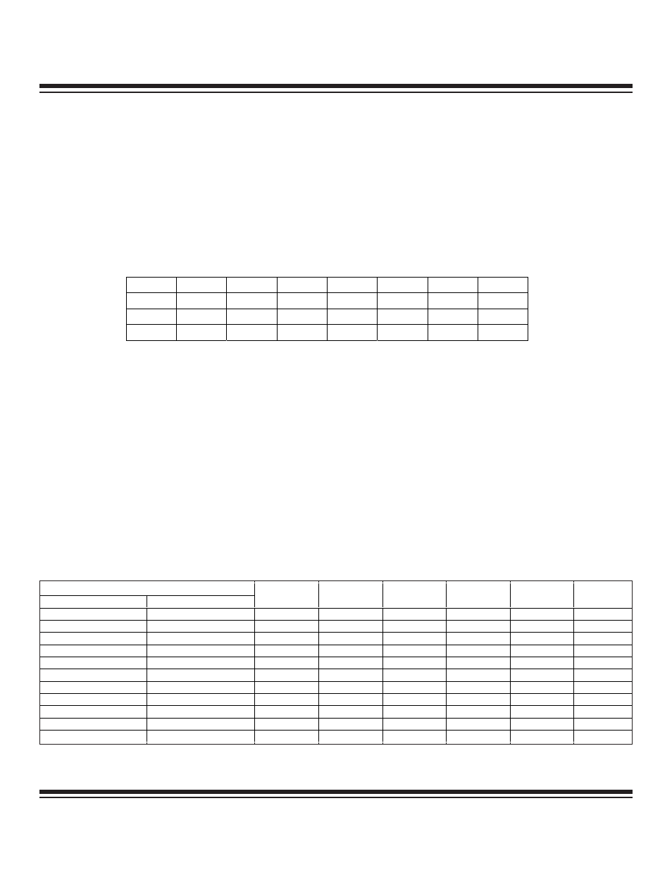
13.2.1 1-Wire Clock Divisor Register (OWA = 100b)
Bit 7: Clock Enable (CLK_EN). The CLK_EN bit of the Clock Divisor register is used to control the clock generation circuitry in the Bus
Master. Setting the CLK_EN bit to logic 1 enables the clock generation circuitry according to the PRE[1:0] and DIV[2:0] settings.
Bits 6 and 5: Reserved
Bits 4, 3, 2: Divider Bits 2:0 (DIV[2:0]). These bits allow further division of the prescaled clock for generating a 1-Wire base clock:
Base Clock = Prescaled Clock / (2
DIV2:0
)
Bits 1 and 0: Clock Prescaler Bits 1:0 (PRE[1:0]). These prescaler bits define the initial clock division applied to the reference clock
input. The prescaled clock output will be according to the following equation:
Prescaled Clock = Reference Clock / (2 x PRE[1:0] + 1)
The Clock Divisor register must be configured properly before any 1-Wire communication can take place. The Bus Master clock divi-
sor settings currently allow reference clock input frequencies between 4MHz and 25MHz with ~50% duty cycle to be supported. Table
13-1 summarizes the proper division values, based upon the reference input clock range. Settings not listed in the table are reserved
and can result in improper operation if used. Note that providing a system clock frequency nearer the minimum of a given reference
clock frequency range yields base-clock frequencies closer to 1MHz and better timing margin.
Table 13-1. Clock Divisor Register Setting for Reference Clock Rates
13-4
MAXQ Family User’s Guide
REFERENCE CLOCK FREQUENCY (MHz)
MIN
MAX
DIVIDER RATIO
DIV2
DIV1
DIV0
PRE1
PRE0
4.0
< 5.0
4
0
1
0
0
0
5.0
< 6.0
5
0
0
0
1
0
6.0
< 7.0
6
0
0
1
0
1
7.0
< 8.0
7
0
0
0
1
1
8.0
< 10.0
8
0
1
1
0
0
10.0
< 12.0
10
0
0
1
1
0
12.0
< 14.0
12
0
1
0
0
1
14.0
< 16.0
14
0
0
1
1
1
16.0
< 20.0
16
1
0
0
0
0
20.0
< 24.0
20
0
1
0
1
0
24.0
≤ 25.0
24
0
1
1
0
1
Bit #
7
6
5
4
3
2
1
0
Name
CLK_EN
—
—
DIV2
DIV1
DIV0
PRE1
PRE0
Reset
0
0
0
0
0
0
0
0
Access
rw
r
r
rw
rw
rw
rw
rw
r = read, w = write
Maxim Integrated
