Cache line, Size, Cache line size – Avago Technologies LSI53C825AE User Manual
Page 96: Cache, Line size, Latency timer, 0x0c, Register: 0x0c, Register: 0x0d
4-8
Registers
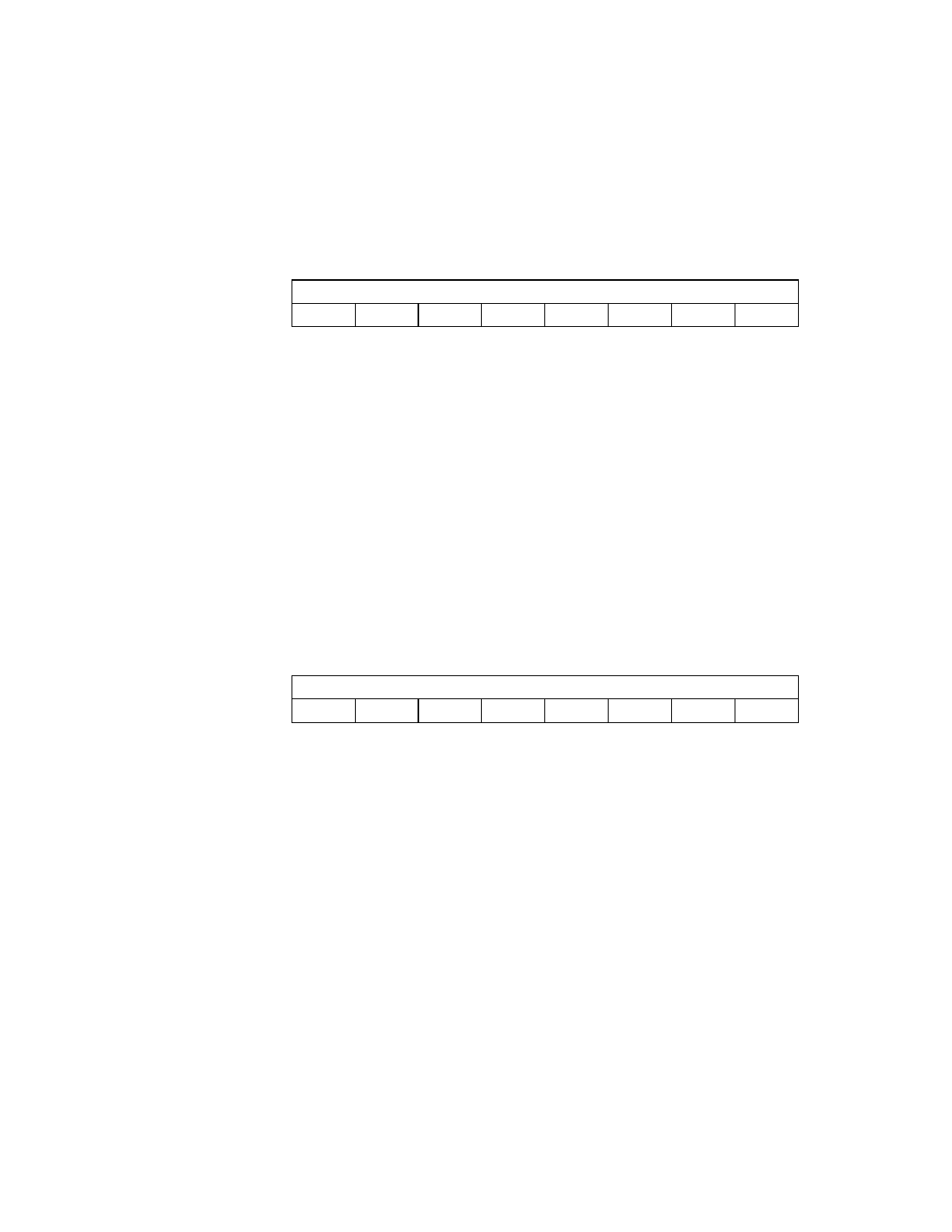
Register: 0x0C
Cache Line Size
Read/Write
CLS
Cache Line Size
[7:0]
This register specifies the system cache line size in units
of 32-bit words. Cache mode is enabled and disabled by
the Cache Line Size Enable (CLSE) bit, bit 7 in the
register. Setting this bit causes the
LSI53C825A to align to cache line boundaries before
allowing any bursting, except during Memory Moves in
which the read and write addresses are not aligned to a
burst size boundary. For more information on this register,
see
Section 2.1.3.1, “Support for PCI Cache Line Size
Register: 0x0D
Latency Timer
Read/Write
LT[7:0]
Latency Timer
[7:0]
The
register specifies, in units of PCI bus
clocks, the value of the Latency Timer for this PCI bus
master. The LSI53C825A supports this timer. All eight
bits are writable, allowing latency values of 0–255 PCI
clocks. Use the following equation to calculate an
optimum latency value for the LSI53C825A:
Latency = 2 + (Burst Size * (typical wait states +1)).
Values greater than optimum are also acceptable.
7
0
CLS
0
0
0
0
0
0
0
0
7
0
LT
0
0
0
0
0
0
0
0