Avago Technologies LSI53C825AE User Manual
Page 140
4-52
Registers
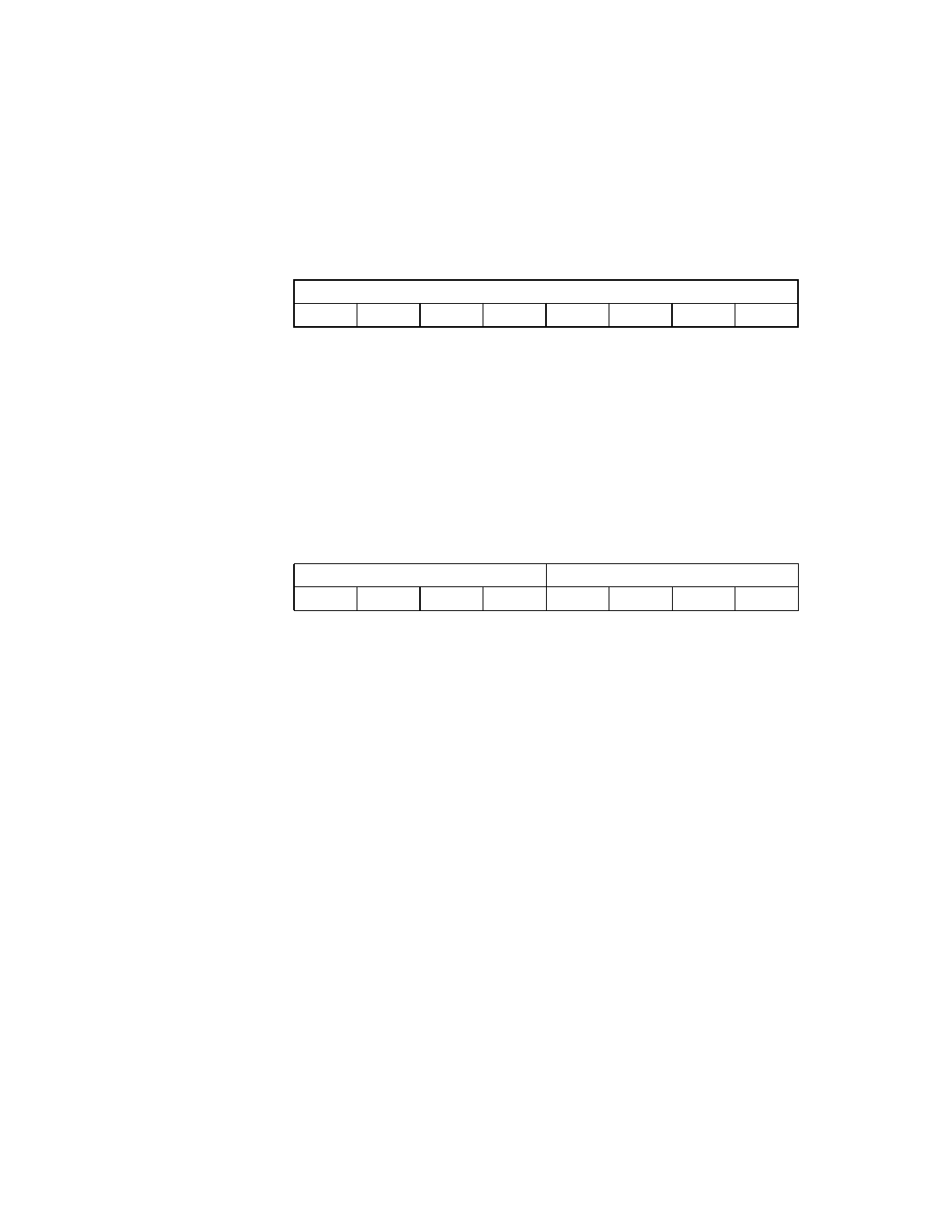
Register: 0x18 (0x98)
Chip Test Zero (CTEST0)
Read/Write
FMT
Byte Empty in DMA FIFO
[7:0]
This was a general purpose read/write register in
previous LSI53C8XX family chips. Although it is still a
read/write register, LSI Logic reserves the right to use
these bits for future LSI53C8XX family enhancements.
Register: 0x19 (0x99)
Chip Test One (CTEST1)
Read Only
FMT[3:0]
Byte Empty in DMA FIFO
[7:4]
These bits identify the bottom bytes in the DMA FIFO that
are empty. Each bit corresponds to a byte lane in the
DMA FIFO. For example, if byte lane three is empty, then
FMT3 is set. Since the FMT flags indicate the status of
bytes at the bottom of the FIFO, if all FMT bits are set,
the DMA FIFO is empty.
FFL[3:0]
Byte Full in DMA FIFO
[3:0]
These status bits identify the top bytes in the DMA FIFO
that are full. Each bit corresponds to a byte lane in the
DMA FIFO. For example, if byte lane three is full then
FFL3 is set. Since the FFL flags indicate the status of
bytes at the top of the FIFO, if all FFL bits are set, the
DMA FIFO is full.
7
0
FMT
1
1
1
1
1
1
1
1
7
0
FMT[3:0]
FFL[3:0]
1
1
1
1
0
0
0
0
- MGA-725M4 (4 pages)
- MGA-71543 (4 pages)
- MGA-71543 (3 pages)
- MGA-82563 (6 pages)
- 3ware SAS 9750-8i (48 pages)
- 3ware 9690SA-8I (Channel) (138 pages)
- 3ware 9690SA-8I (Channel) (380 pages)
- 3ware SAS 9750-8i (29 pages)
- 3ware 9550SXU-8LP (Channel) (149 pages)
- 3ware 9550SXU-8LP (Channel) (40 pages)
- 3ware 9650SE-8LPML (Channel) (45 pages)
- 3ware 9690SA-8I (Channel) (27 pages)
- 3ware 9690SA-8I (Channel) (361 pages)
- 6160 SAS Switch (2 pages)
- Cache Protection for RAID Controller Cards (13 pages)
- MegaRAID SAS 9271-8iCC (13 pages)
- MegaRAID SAS 9361-8i (13 pages)
- MegaRAID SAS 9266-8i (12 pages)
- MegaRAID SAS 9380-8e (43 pages)
- Cache Protection for RAID Controller Cards (139 pages)
- MegaRAID SAS 9285-8ecv (80 pages)
- MegaRAID SAS 9285-8ecv (92 pages)
- MegaRAID SAS 9266-8i (20 pages)
- MegaRAID SAS 9271-8iCC (26 pages)
- MegaRAID SafeStore Software (502 pages)
- MegaRAID SAS 0260CV-4i (72 pages)
- MegaRAID SAS 0260CV-4i (64 pages)
- MegaRAID SAS 0260CV-4i (49 pages)
- MegaRAID SAS 9271-8i (8 pages)
- MegaRAID SAS 9361-8i (7 pages)
- MegaRAID SAS 9341-8i (8 pages)
- MegaRAID SAS 9380-4i4e (7 pages)
- MegaRAID SAS 9380-8e (7 pages)
- MegaRAID SAS 0260CV-4i (28 pages)
- MegaRAID SAS 9240-8i (4 pages)
- MegaRAID SAS 9280-24i4e (16 pages)
- MegaRAID SAS 9260-16i (12 pages)
- MegaRAID SAS 9280-24i4e (14 pages)
- MegaRAID SAS 9260-8i (4 pages)
- MegaRAID SafeStore Software (8 pages)
- MegaRAID SAS 9280-8e (22 pages)
- MegaRAID SAS 9261-8i (4 pages)
- MegaRAID SAS 9285-8e (12 pages)
- MegaRAID SAS 9280-16i4e (12 pages)
- MegaRAID SAS 9280-4i4e (4 pages)