Chip test two (ctest2), Chip test two, Ctest2) – Avago Technologies LSI53C825AE User Manual
Page 141: Register: 0x1a (0x9a)
Operating Registers
4-53
Register: 0x1A (0x9A)
Chip Test Two (CTEST2)
Read/Write
DDIR
Data Transfer Direction
7
This status bit indicates which direction data is being
transferred. When this bit is set, the data is transferred
from the SCSI bus to the host bus. When this bit is clear,
the data is transferred from the host bus to the SCSI bus.
SIGP
Signal Process
6
This bit is a copy of the SIGP bit in the
register (bit 5). The SIGP bit is used to signal a
running SCRIPTS instruction. When this register is read,
the SIGP bit in the ISTAT0 register is cleared.
CIO
Configured as I/O
5
This bit is defined as the Configuration I/O Enable Status
bit. This read only bit indicates if the chip is currently
enabled as I/O space.
Note:
Bits 4 and 5 may be set if the chip is dual-mapped.
CM
Configured as Memory
4
This bit is defined as the configuration memory enable
status bit. This read only bit indicates if the chip is
currently enabled as memory space.
Note:
Bits 4 and 5 may be set if the chip is dual-mapped.
SRTCH
SCRATCHA/B Operation
3
This bit controls the operation of the
and
registers. When it is set, SCRATCHB contains the RAM
base address value from the PCI configuration RAM
Base Address register. This is the base address for the
4 Kbyte internal RAM. In addition, the
register displays the memory-mapped
based address of the chip operating registers. When this
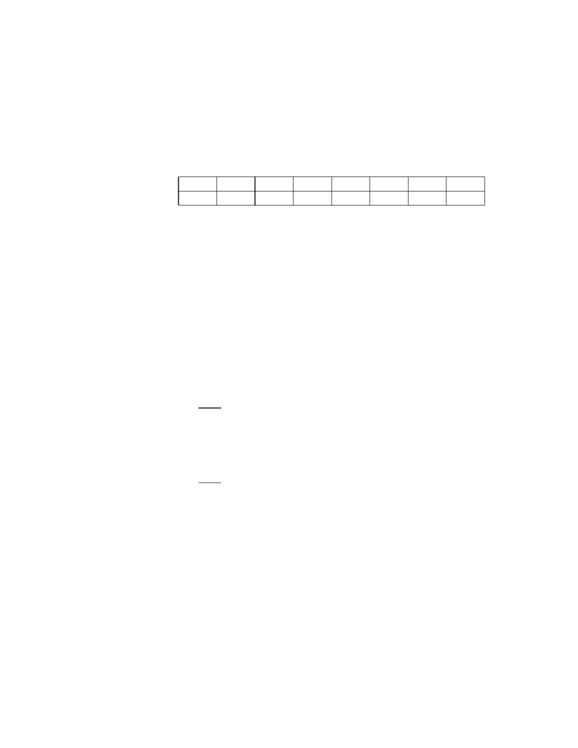
7
6
5
4
3
2
1
0
DDIR
SIGP
CIO
CM
SRTCH
TEOP
DREQ
DACK
0
0
x
x
0
0
0
1