9 jtag signals, 2 mad bus programming, Jtag signals – Avago Technologies LSI53C825AE User Manual
Page 85: Mad bus programming, Jtag signals (lsi53c825aj, lsi53c825aje only), Table 3.10, Section 3.2, “mad bus programming
MAD Bus Programming
3-15
3.1.9 JTAG Signals
describes the signals for the JTAG Signals group:
3.2 MAD Bus Programming
The MAD[7:0] pins, in addition to serving as the address/data bus for the
local memory interface, are also used to program power-up options for
the chip. A particular option is programmed by connecting a 4.7 k
Ω
resistor between the appropriate MAD(x) pin and Vss. The pull-down
resistors require that HC or HCT external components are used for a
memory interface.
•
MAD[7] – has no functionality. Do not place a pull-down resistor on
this pin.
•
MAD[6] – Subsystem Data configuration. Please refer to the
for the different configurations.
•
MAD[5] – SCRIPTS RAM disable. Connecting a 4.7 k
Ω
resistor
between MAD[5] and Vss disables SCRIPTS RAM.
•
MAD[4] – Subsystem Data configuration. Please refer to the
and
below for the different configurations.
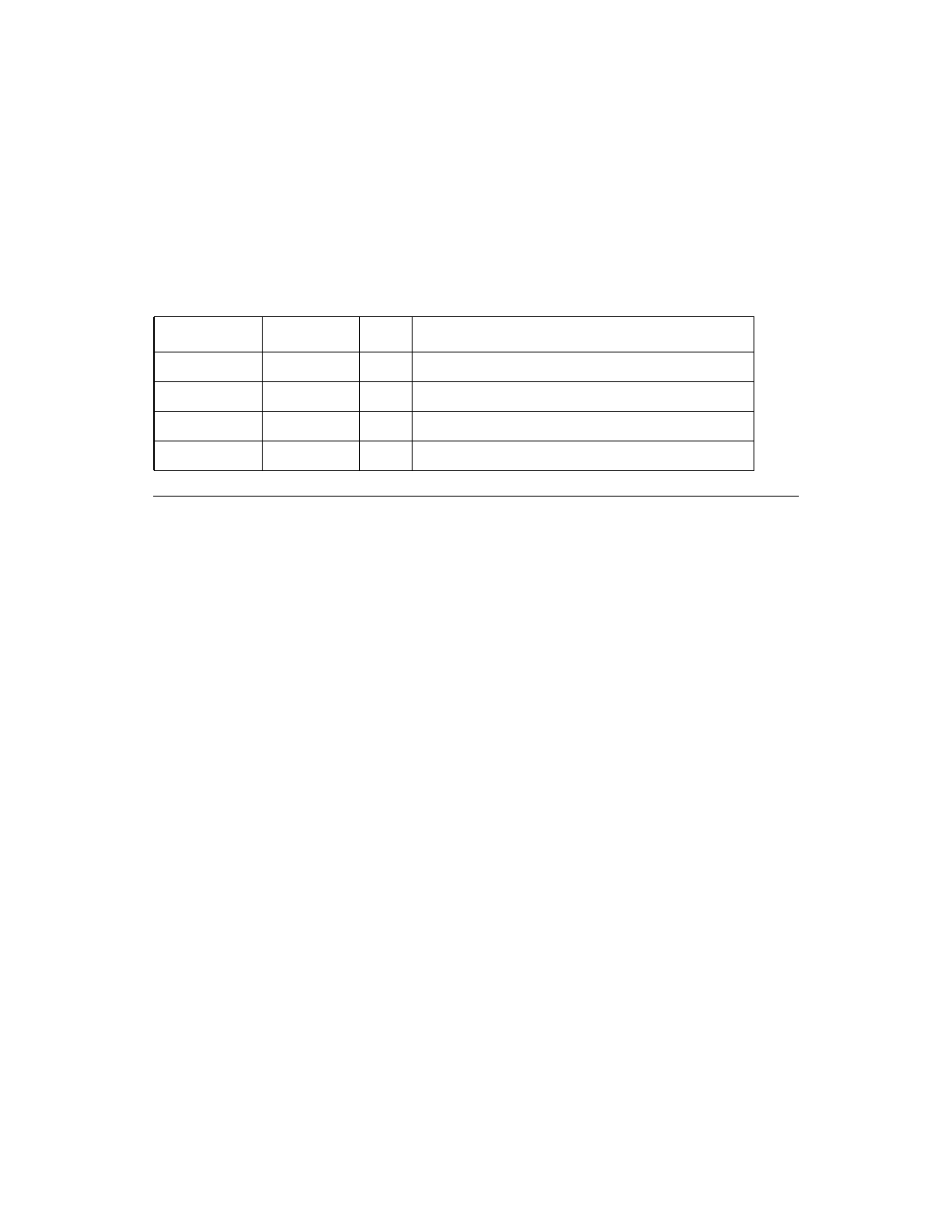
Table 3.10
JTAG Signals (LSI53C825AJ, LSI53C825AJE Only)
Name
Pin No.
Type
Description
TCK
130/130
–
Test Clock pin for JTAG boundary scan.
TMS
57/57
–
Test Mode Select pin for JTAG boundary scan.
TDI
142/142
–
Test Data In pin for JTAG boundary scan.
TDO
58/58
–
Test Data Out pin for JTAG boundary scan.