Dma mode (dmode), Dma mode, Dmode) – Avago Technologies LSI53C825AE User Manual
Page 153: Scratch register a, Scratcha), Scratch register a (scratcha), Mode (dmode), 0x38 (0xb8)
Operating Registers
4-65
Registers: 0x34–0x37 (0xB4–0xB7)
Scratch Register A (SCRATCHA)
Read/Write
SCRATCHA
Scratch Register A
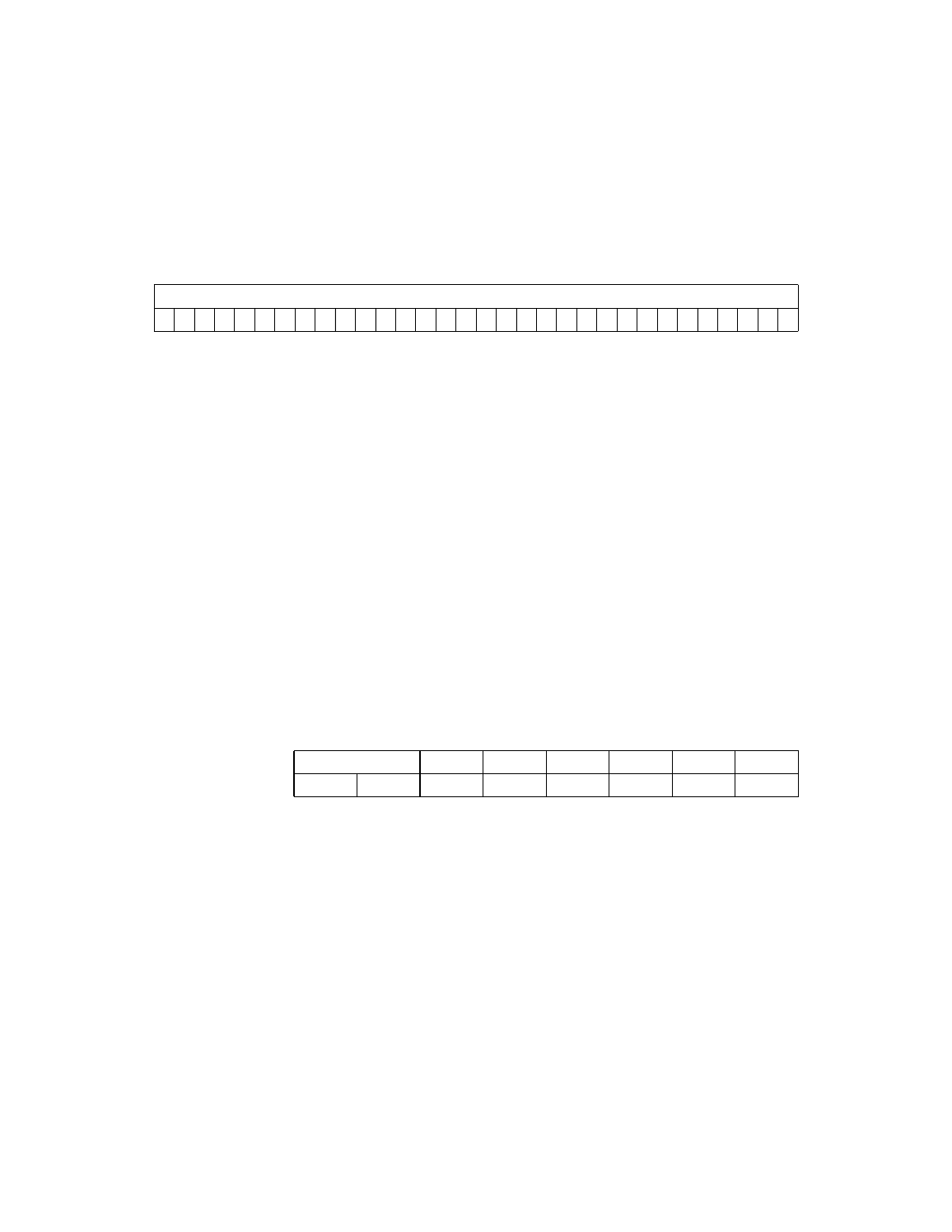
[31:0]
This is a general purpose, user-definable scratch pad
register. Apart from CPU access, only register read/write
and memory moves into the SCRATCH register alter its
contents. The LSI53C825A cannot fetch SCRIPTS
instructions from this location. When bit 3 in the
register is set, this register contains the
memory mapped base address of the operating registers.
Setting
, bit 3 only causes the
base address to appear in this register; any information
that was previously in the register will remain intact. Any
writes to this register while
, bit 3
is set will pass through to the actual
register. The power-up value of this
register is indeterminate.
Register: 0x38 (0xB8)
DMA Mode (DMODE)
Read/Write
BL[1:0]
Burst Length
[7:6]
These bits control the maximum number of Dwords
transferred per bus ownership, regardless of whether the
transfers are back-to-back, burst, or a combination of
both. This value is also independent of the width (64 or
32 bits) of the data transfer on the PCI bus. The
LSI53C825A asserts the Bus Request (REQ/) output
when the DMA FIFO can accommodate a transfer of at
least one burst threshold of data. Bus Request (REQ/) is
also asserted during start-of-transfer and end-of-transfer
cleanup and alignment, even if less than a full burst of
31
0
SCRATCHA
x
x
x
x
x
x
x
x
x
x
x
x
x
x
x
x
x
x
x
x
x
x
x
x
x
x
x
x
x
x
x
x
7
6
5
4
3
2
1
0
BL[1:0]
SIOM
DIOM
ER
ERMP
BOF
MAN
0
0
0
0
0
0
0
0