Dma fifo (dfifo), Dma fifo, Dfifo) – Avago Technologies LSI53C825AE User Manual
Page 144
4-56
Registers
Registers: 0x1C–0x1F (0x9C–0x9F)
Temporary (TEMP)
Read/Write
TEMP
Temporary
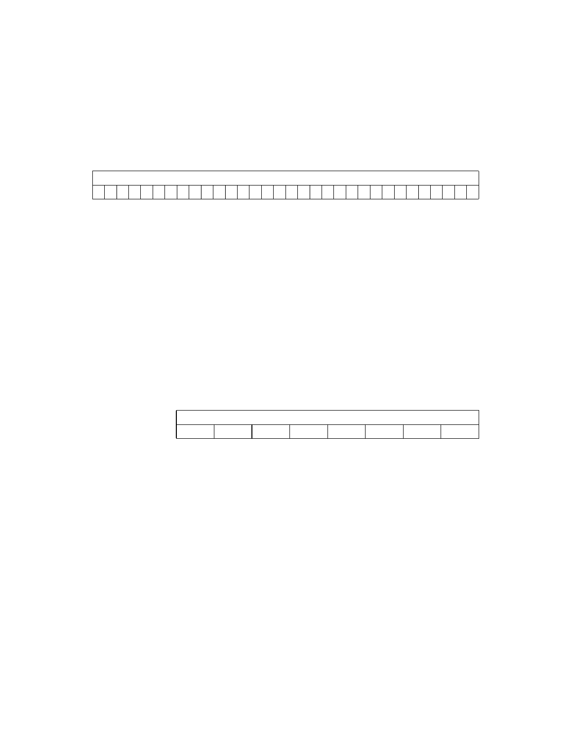
[31:0]
This 32-bit register stores the Return instruction address
pointer from the Call instruction. The address pointer
stored in this register is loaded into the
register when a Return instruction is
executed. This address points to the next instruction to
execute. Do not write to this register while the
LSI53C825A is executing SCRIPTS.
During any Memory-to-Memory Move operation, the
contents of this register are preserved. The power-up
value of this register is indeterminate.
Register: 0x20 (0xA0)
DMA FIFO (DFIFO)
Read/Write
BO
Byte Offset Counter
[7:0]
These bits, along with bits [1:0] in the
register, indicate the amount of data
transferred between the SCSI core and the DMA core. It
is used to determine the number of bytes in the DMA
FIFO when an interrupt occurs. These bits are unstable
while data is being transferred between the two cores.
Once the chip has stopped transferring data, these bits
are stable.
The
register counts the number of
bytes transferred between the DMA core and the SCSI
core. The
register counts the
number of bytes transferred across the host bus. The
31
0
TEMP
x
x
x
x
x
x
x
x
x
x
x
x
x
x
x
x
x
x
x
x
x
x
x
x
x
x
x
x
x
x
x
x
7
0
BO
x
0
0
0
0
0
0
0