1 pci bus interface signals, 1 system signals, Table 3.2 system signals – Avago Technologies LSI53C825AE User Manual
Page 76: Pci bus interface signals, System signals, Section 3.1, “pci bus interface signals
3-6
Signal Descriptions
3.1 PCI Bus Interface Signals
The PCI Bus Interface Signals section contains tables describing the
signals for the following signal groups:
,
,
External Memory Interface Signals
, and
3.1.1 System Signals
describes the signals for the System Signals group:
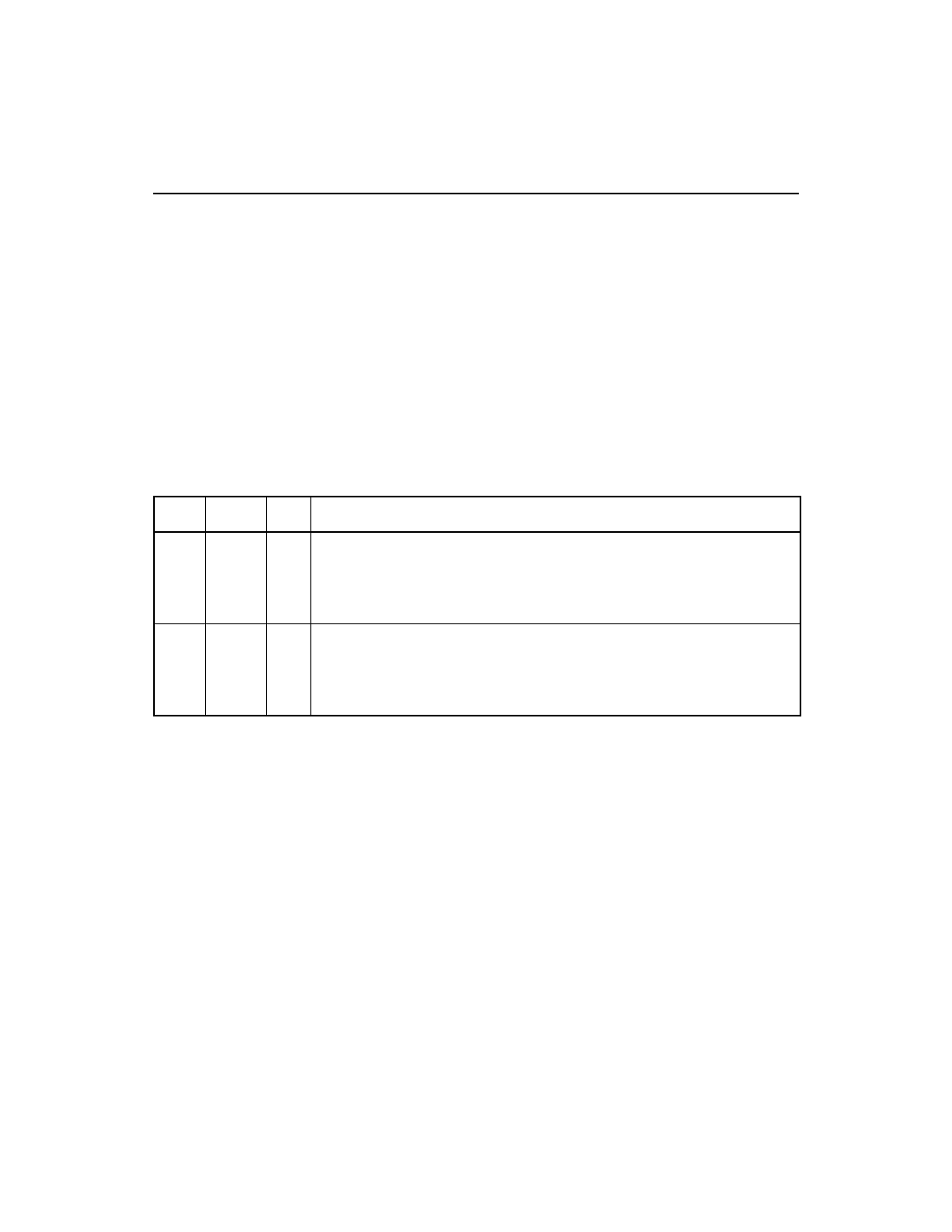
Table 3.2
System Signals
Name
Pin No. Type Description
CLK
145
I
Clock provides timing for all transactions on the PCI bus and is an input to
every PCI device. All other PCI signals are sampled on the rising edge of
CLK, and other timing parameters are defined with respect to this edge. This
clock can optionally be used as the SCSI core clock; however, the
LSI53C825A is not able to achieve Fast SCSI transfer rates.
RST/
144
I
Reset forces the PCI sequencer of each device to a known state. All t/s and
s/t/s signals are forced to a high impedance state, and all internal logic is
reset. The RST/ input is synchronized internally to the rising edge of CLK.
The CLK input must be active while RST/ is active to properly reset the
device.