Dma control, Dcntl), Dma control (dcntl) – Avago Technologies LSI53C825AE User Manual
Page 157: Control (dcntl), Dma con, Trol (dcntl), Register: 0x3a (0xba), Register: 0x3b (0xbb)
Operating Registers
4-69
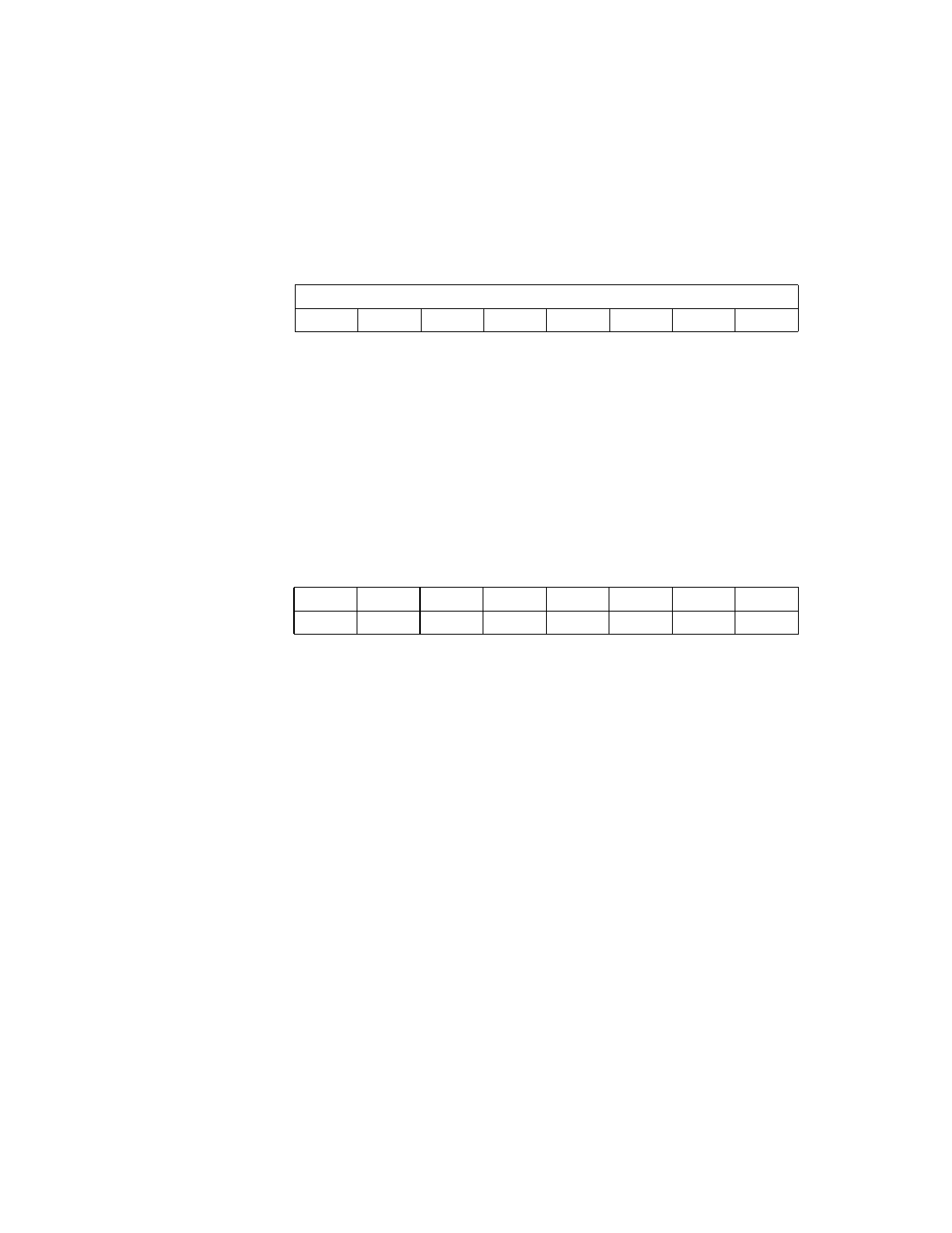
Register: 0x3A (0xBA)
Scratch Byte Register (SBR)
Read/Write
SBR
Scratch Byte Register
[7:0]
This is a general purpose register. Apart from CPU
access, only register read/write and memory moves into
this register alter its contents. The default value of this
register is zero. This register is called the DMA Watchdog
Timer on previous LSI53C8XX family products.
Register: 0x3B (0xBB)
DMA Control (DCNTL)
Read/Write
CLSE
Cache Line Size Enable
7
Setting this bit enables the LSI53C825A to sense and
react to cache line boundaries set up by the
or PCI
register, whichever
contains the smaller value. Clearing this bit disables the
cache line size logic and the LSI53C825A monitors the
cache line size using the
register.
PFF
Prefetch Flush
6
Setting this bit causes the prefetch unit to flush its
contents. This bit clears after the flush is complete.
PFEN
Prefetch Enable
5
Setting this bit enables the prefetch unit if the burst size
is equal to or greater than four. For more information on
SCRIPTS instruction prefetching, see
7
0
SBR
0
0
0
0
0
0
0
0
7
6
5
4
3
2
1
0
CLSE
PFF
PFEN
SSM
IRQM
STD
IRQD
COM
0
0
0
0
0
0
0
0