Figure3.3 lsi53c825a functional signal grouping, Lsi53c825a functional signal grouping, Figure 3.3 – Avago Technologies LSI53C825AE User Manual
Page 75
3-5
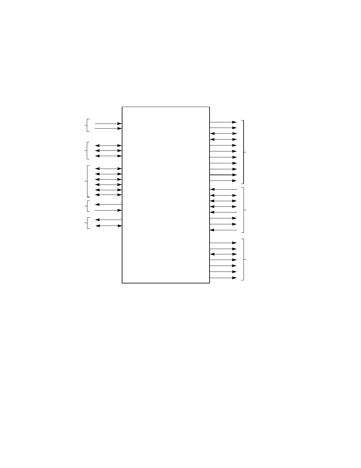
is the functional signal grouping for the LSI53C825A.
Figure 3.3
LSI53C825A Functional Signal Grouping
LSI53C825A
CLK
RST
AD[31:0]
C_BE/[3:0]
PAR
FRAME/
TRDY/
IRDY/
STOP/
DEVSEL/
IDSEL
REQ/
GNT/
SERR/
PERR/
TGS
GPIO[4:3]
GPIO0_FETCH/
GPIO1_MASTER/
MAC/_TESTOUT
IRQ/
BIG_LIT/
DIFFSENS
GPIO2_MAS2/
MWE/
MCE/
MOE/
MAS0/
System
Address
and
Data
Interface
Control
Arbitration
Error
Reporting
SCSI
MAS1/
BSYDIR
RSTDIR
SELDIR
IGS
SDIRP[1:0]
SDIR[15:0]
SCLK
SD[15:0]
SDP[1:0]
SCTRL
Additional
MAD[7:0]
TESTIN/
Device Local
Memory Bus
and Control
Interface
See also other documents in the category Avago Technologies Hardware:
- MGA-725M4 (4 pages)
- MGA-71543 (4 pages)
- MGA-71543 (3 pages)
- MGA-82563 (6 pages)
- 3ware SAS 9750-8i (48 pages)
- 3ware 9690SA-8I (Channel) (138 pages)
- 3ware 9690SA-8I (Channel) (380 pages)
- 3ware SAS 9750-8i (29 pages)
- 3ware 9550SXU-8LP (Channel) (149 pages)
- 3ware 9550SXU-8LP (Channel) (40 pages)
- 3ware 9650SE-8LPML (Channel) (45 pages)
- 3ware 9690SA-8I (Channel) (27 pages)
- 3ware 9690SA-8I (Channel) (361 pages)
- 6160 SAS Switch (2 pages)
- MegaRAID SAS 9380-8e (43 pages)
- Cache Protection for RAID Controller Cards (139 pages)
- Cache Protection for RAID Controller Cards (13 pages)
- MegaRAID SAS 9271-8iCC (13 pages)
- MegaRAID SAS 9361-8i (13 pages)
- MegaRAID SAS 9266-8i (12 pages)
- MegaRAID SAS 9266-8i (20 pages)
- MegaRAID SAS 9271-8iCC (26 pages)
- MegaRAID SafeStore Software (502 pages)
- MegaRAID SAS 9285-8ecv (80 pages)
- MegaRAID SAS 9285-8ecv (92 pages)
- MegaRAID SAS 0260CV-4i (49 pages)
- MegaRAID SAS 9271-8i (8 pages)
- MegaRAID SAS 0260CV-4i (72 pages)
- MegaRAID SAS 0260CV-4i (64 pages)
- MegaRAID SAS 9361-8i (7 pages)
- MegaRAID SAS 9341-8i (8 pages)
- MegaRAID SAS 9380-4i4e (7 pages)
- MegaRAID SAS 9380-8e (7 pages)
- MegaRAID SAS 0260CV-4i (28 pages)
- MegaRAID SAS 9240-8i (4 pages)
- MegaRAID SAS 9280-24i4e (14 pages)
- MegaRAID SAS 9280-24i4e (16 pages)
- MegaRAID SAS 9260-16i (12 pages)
- MegaRAID SAS 9260-8i (4 pages)
- MegaRAID SafeStore Software (8 pages)
- MegaRAID SAS 9280-8e (22 pages)
- MegaRAID SAS 9261-8i (4 pages)
- MegaRAID SAS 9285-8e (12 pages)
- MegaRAID SAS 9280-16i4e (12 pages)
- MegaRAID SAS 9280-4i4e (4 pages)