Chip test four (ctest4), Chip test four, Ctest4) – Avago Technologies LSI53C825AE User Manual
Page 145
Operating Registers
4-57
difference between these two counters represents the
number of bytes remaining in the DMA FIFO.
The following steps determine how many bytes are left in
the DMA FIFO when an error occurs, regardless of the
transfer direction:
Step 1. If the DMA FIFO size is set to 88 bytes, subtract
the seven least significant bits of the
register from the 7-bit value of
the
register.
If the DMA FIFO size is set to 536 bytes (using bit 5 of
the
register), subtract the
10 least significant bits of the
register from the 10-bit value of the DMA FIFO Byte
offset Counter, which consists of bits [1:0] in the
register and bits [7:0] of the
register.
Step 2. If the DMA FIFO size is set to 88 bytes, AND the
result with 0x7F for a byte count between zero
and 64. If the DMA FIFO size is set to 536 bytes,
AND the result with 0x3FF for a byte count
between zero and 536.
Note:
If trying to calculate the total number of bytes in both the
DMA FIFO and SCSI logic, see
in
Chapter 2, “Functional Description.”
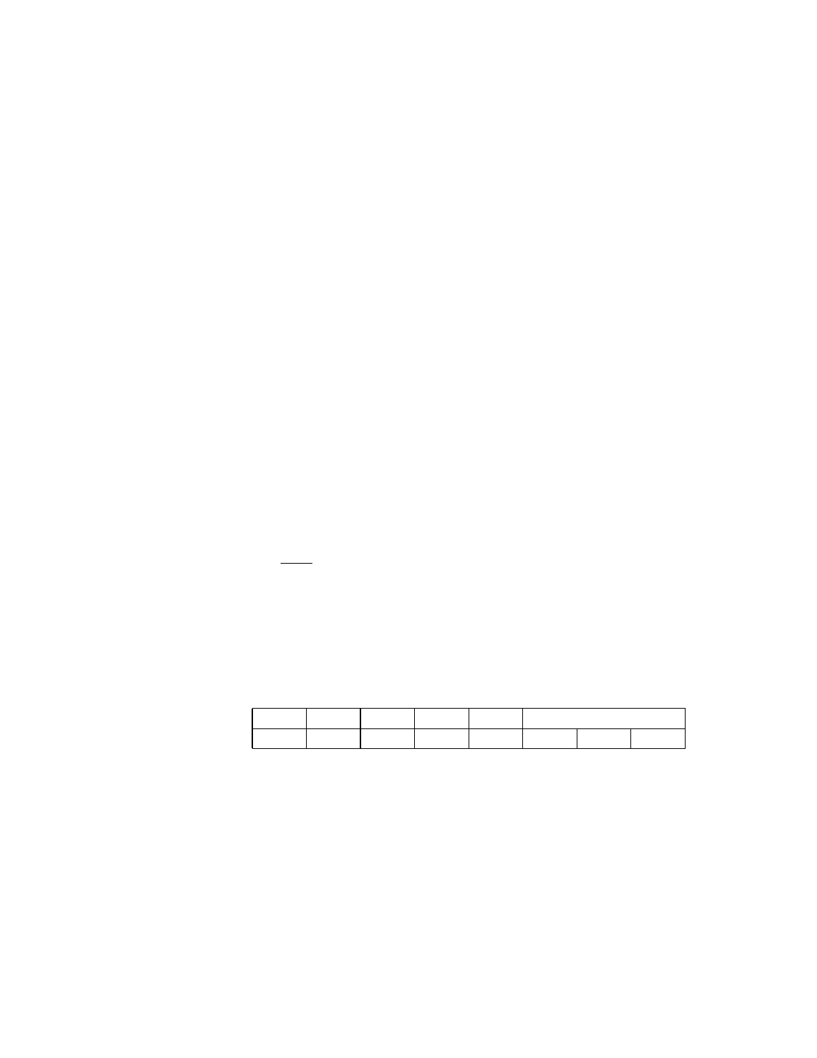
Register: 0x21 (0xA1)
Chip Test Four (CTEST4)
Read/Write
BDIS
Burst Disable
7
When set, this bit causes the LSI53C825A to perform
back to back cycles for all transfers. When this bit is
cleared, back to back transfers for opcode fetches and
burst transfers for data moves are performed.
7
6
5
4
3
2
0
BDIS
ZMOD
ZSD
SRTM
MPEE
FBL[2:0]
0
0
0
0
0
0
0
0