3 pcmcia interface timing diagrams and parameters, Pcmcia voltage-control logic -31, Figure 10-14 – Intel STRONGARM SA-1100 User Manual
Page 145

SA-1100 Developer’s Manual
10-31
Memory and PCMCIA Control Module
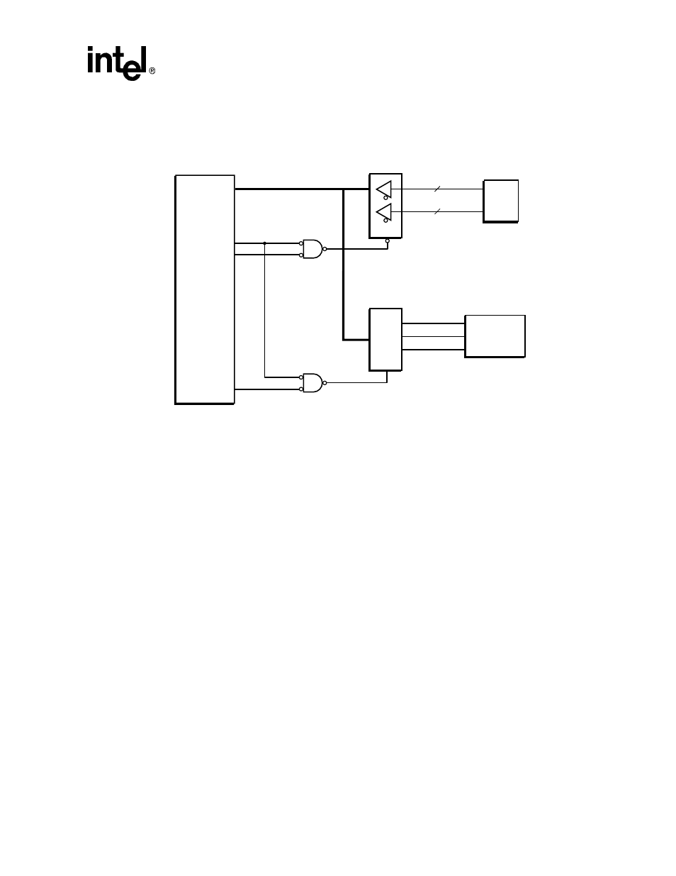
Figure 10-14. PCMCIA Voltage-Control Logic
The PCMCIA card voltage may be controlled through a set of discrete registers mapped into a
static chip select. For example,
shows mapping to chip select 3.
10.6.3
PCMCIA Interface Timing Diagrams and Parameters
shows a 16-bit access to a 16-bit memory or I/O device. The parameter, BS, is
programmed in the MECR register. When common memory is accessed, the MECR:BSM1 or
MECR:BSM2 field is used, depending on whether card socket 0 or 1 is addressed.
MECR:BSIO1(2) is used for I/O accesses and MECR:BSA1(2) is used for access to attribute
memory.
show the appropriate setting of BS_xx = 0b00001.
A6845-01
D<15:0>
nWE
Socket x
nCS<3>
nOE
EN#
WR
Transparent
Latch
VPPEN
3VEN
5VEN
2
2
VSS 1,2
BVD 1,2
Voltage-Control
Circuit
Intel
®
StrongARM
®*
SA-1100
* StrongARM is a registered trademark of ARM Limited.
