3 sram interface overview, 4 sram timing diagrams and parameters, Sram write timing diagram (4–beat burst) -22 – Intel STRONGARM SA-1100 User Manual
Page 136

10-22
SA-1100
Developer’s Manual
Memory and PCMCIA Control Module
10.4.3
SRAM Interface Overview
The SA-1100 provides a 32-bit asynchronous SRAM interface that uses the nCAS pins for byte
selects on both reads and writes (nCS<3:0> selects the SRAM bank, nOE is asserted on reads, and
nWE is asserted on writes). Address bits A<25:2> provide addressability of up to 64 Mbyte of
SRAM per bank. Because the nCAS signals are used to access SRAM, a system with both SRAM
and DRAM is not supported.
The timing for a read access is identical to that for a nonburst ROM. (See
.) The RDF fields in the MSCx registers are the latency for a read access. The MSCx:RDN field
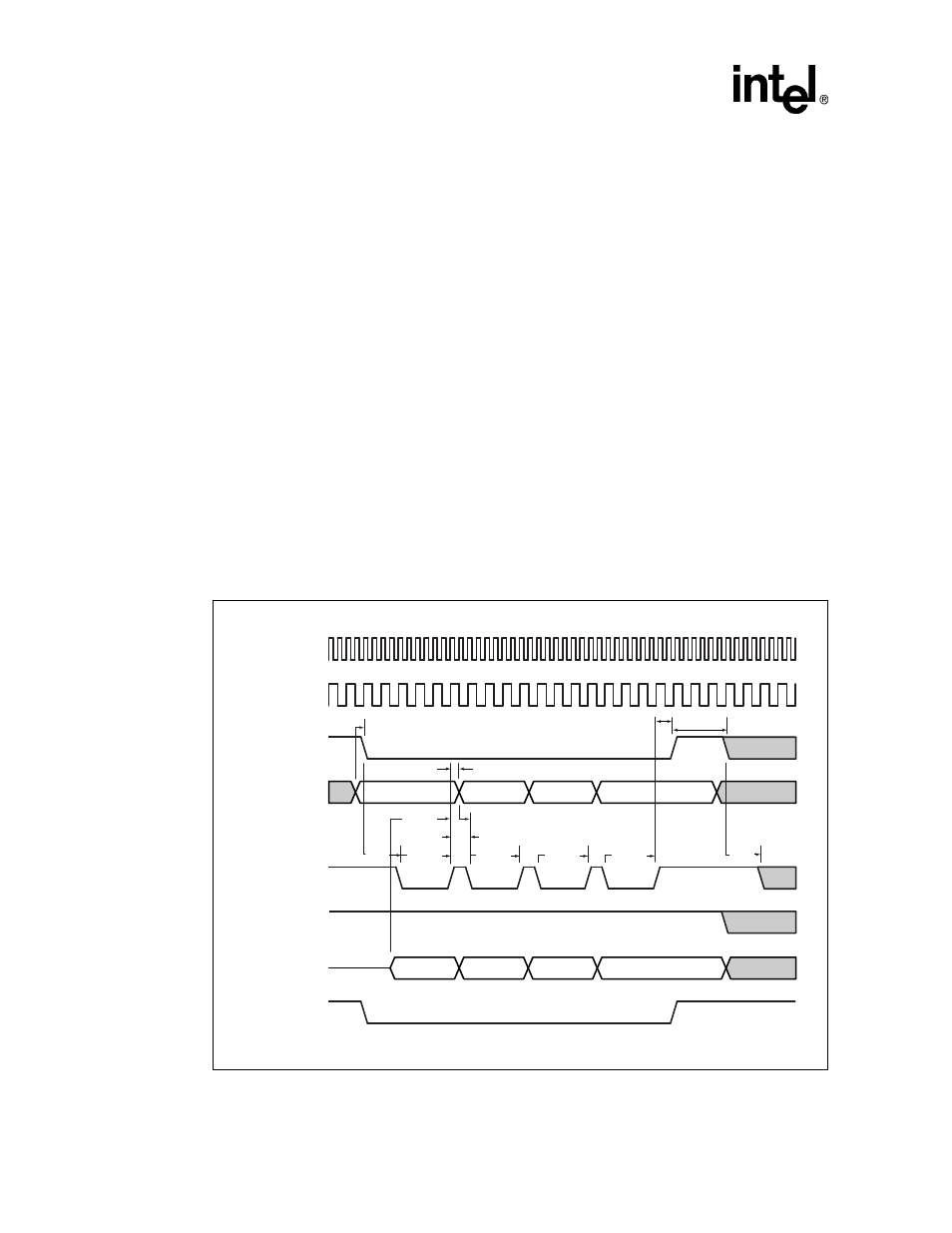
controls the nWE low time during a write cycle. MSCx:RRR is the time from nCS deassertion after
a read to the start of an access from a different memory bank or after a write to any other memory
access. MSCx:RBW must be set to be a 32-bit bus and MSCx:RT must select SRAM.
10.4.4
SRAM Timing Diagrams and Parameters
SRAM reads have the same timing as nonburst ROMs as shown in
, except nCAS<3:0>
are byte selects and are asserted with the same timing as nCS. When nCAS0 is low (asserted),
D<7:0> will be used to transfer data. When nCAS1 is low, D<15:8> is used, and so on. During
writes, all 32 data pins are actively driven by the SA-1100; they are not tristated regardless of the
state of the individual nCAS pins.
shows the timing for SRAM writes.
Figure 10-9. SRAM Write Timing Diagram (4–Beat Burst)
A4786-01
CPU Clock
Memory Clock
tAS
tDSWH
tASW
tDH
RDN+1
tCES
tCEH
(2*RRR)+1
nCS0
A[25:0]
D[31:0]
nCAS[3:0]
nWE
nOE
A0
D0
D1
D2
D3
A0+4
tAH
A0+8
A0+12
RDN+1
RDN+1
RDN+1
tCES
