3 scc cell register overview, 4 write registers, Scc cell register overview write registers – Zilog Z16C35 User Manual
Page 95
ISCC
User Manual
UM011002-0808
89
5.3 SCC CELL REGISTER OVERVIEW
The SCC cell write register set in each channel includes ten control registers (among them
is the transmit buffer), two sync character registers and two baud rate time constant regis-
ters. The interrupt control register and the master interrupt control and reset register are
shared by both channels.
The only variation in register definition is between the multiplexed and non-multiplexed
bus mode programming of the ISCC. The variation exists in the command decode struc-
ture; register WR0. The following sections describe in detail each write register and the
associated bit configuration for each.
5.4 WRITE REGISTERS
The following sections describe WR registers in detail.
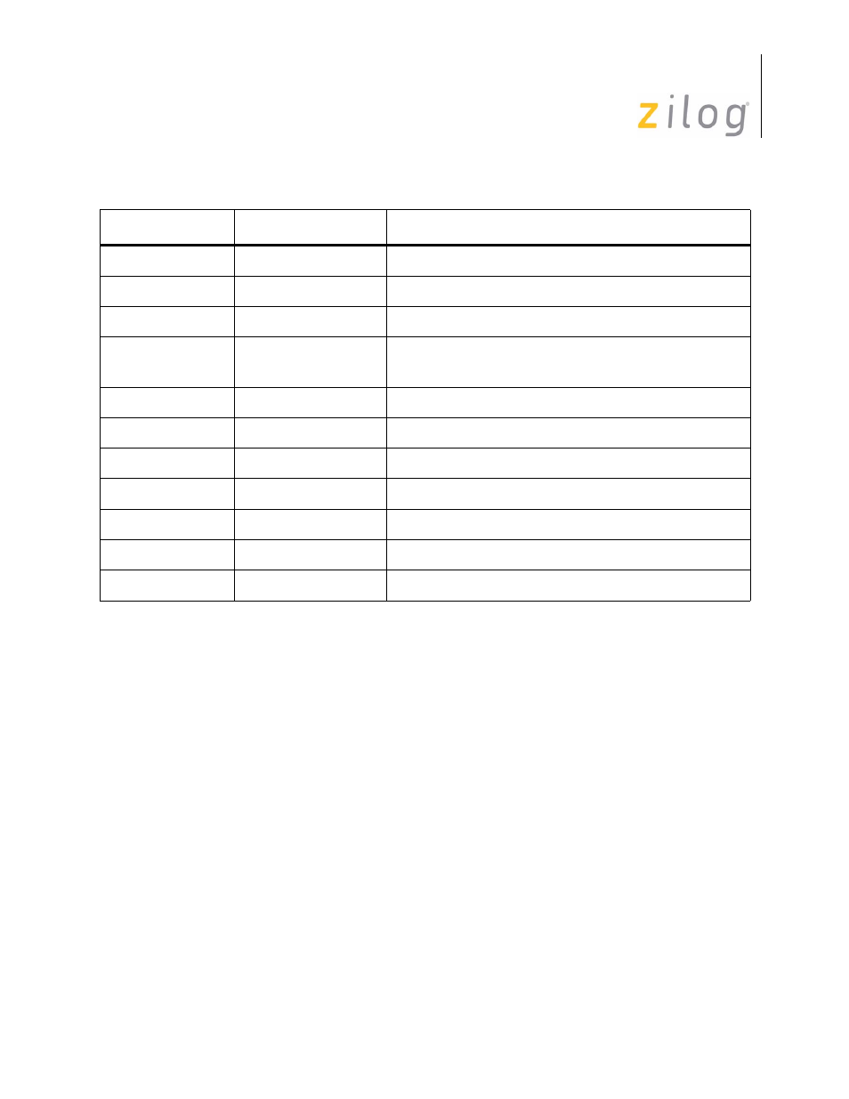
00101
DCR
DMA Control Register
00110 Reserved
Address
00111 Reserved
Address
01000-01001
RDCRA
Receive DMA Count Register Channel A (Low-
high byte)
01010-01011 TDCRA
Transmit
DMA
Count Register Channel A
01100-01101
RDCRB
Receive DMA Count Register Channel B
01110-01111 TDCRB
Transmit
DMA Count Register Channel B
10000-10011
RDARA
Receive DMA Address Register Channel A
10100-10111 TDARA
Transmit
DMA
Address Register Channel A
11000-11011
RDARB
Receive DMA Address Register Channel B
11100-11111 TDARB
Transmit
DMA
Address Register Channel B
Table 5–25. DMA Cell Register Description
Address
Name
Description
Page 89 of 316