Using epld, The z180™ interfaced with the scc at mhz – Zilog Z16C35 User Manual
Page 196

Application Note
The Z180™ Interfaced with the SCC at MHZ
7
The primary chip in this logic is the Shift register (HCT164),
which generates /INTACK, /SCCRD and /WAIT. During
I/O and normal memory access cycles, the Shift Register
(HCT164) remains cleared because the /M1 signal is
inactive during the opcode fetch cycle. Since the Shift
Register output is Low, control of /SCCRD and /WAIT is by
other system logic and gated through the NOR gate
(HCT27). During I/O and normal memory access cycles,
/SCCRD and /SCCWR are generated from the system /RD
and /WR signals, respectively. The generation is by the
logic at the top of Figure 15.
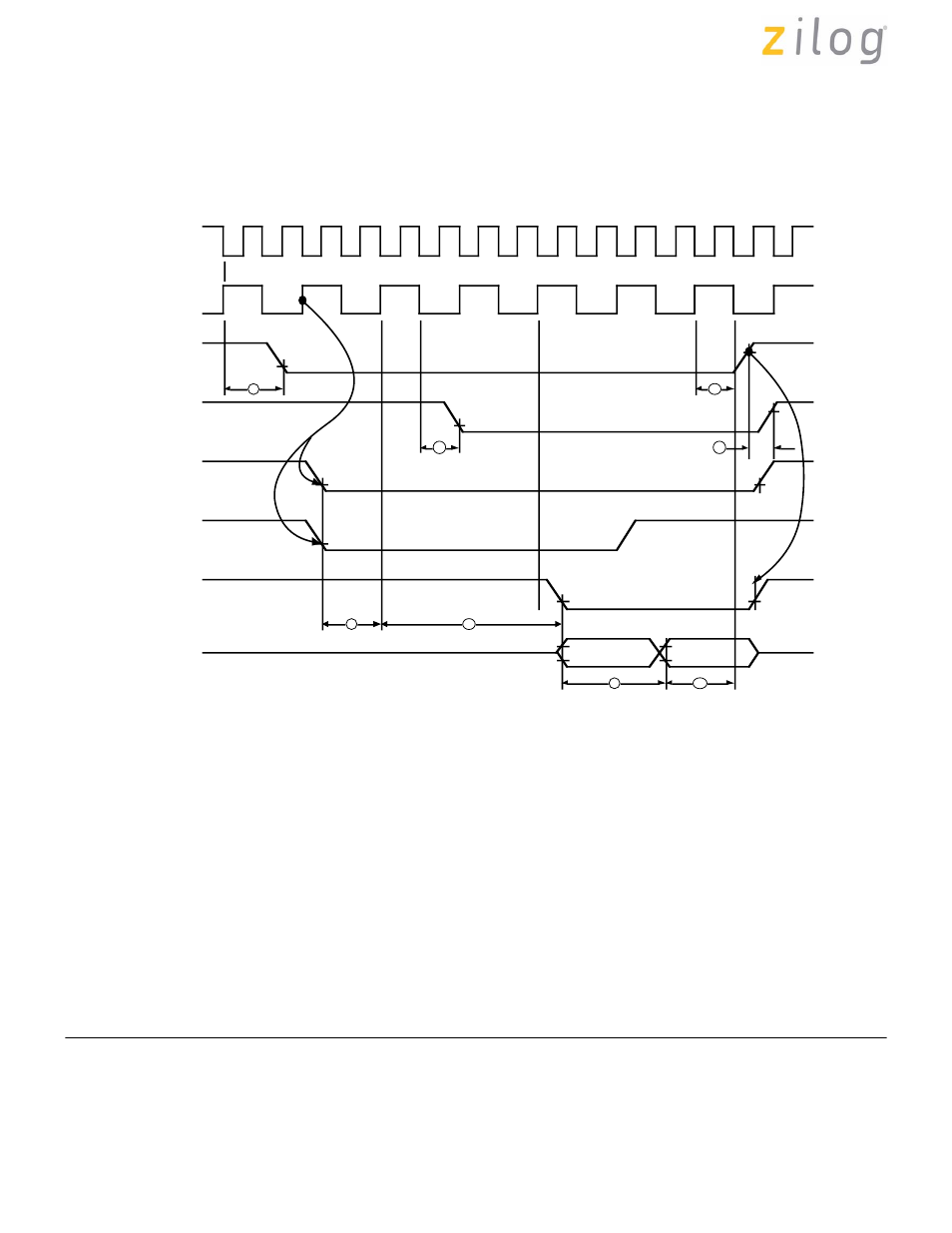
Normally, an Interrupt Acknowledge cycle appears from
the Z180 during /M1 and /IORQ active (which is detected
on the third rising edge of PHI after T1). To get an early
sign of an Interrupt Acknowledge cycle, the Shift register
decodes an active /M1. This is during the presence of an
inactive /MREQ on the rising edge of T2.
During an Interrupt Acknowledge cycle, the /INTACK
signal is generated on the rising edge of T2. Since it is the
presence of /INTACK and an active SCCRD that gates the
interrupt vector onto the data bus, the logic also generates
/SCCRD at the proper time. The timing parameter of
concern here is TdIAi(RD) [/INTACK to /RD
(Acknowledge) Low delay]. This time delay allows the
interrupt daisy chain to settle so the device requesting the
interrupt places its interrupt vector onto the data bus.
The Shift Register allows enough time delay from the
generation of /INTACK before it generates /SCCRD.
During this delay, it places the Z180 into a Wait state until
the valid interrupt vector is placed onto the data bus. If the
time between these two signals is not enough for daisy
chain settling, more time is added by taking /SCCRD and
/WAIT from a later position on the Shift Register. If there is
a requirement for more wait states, the time is calculated
by PHI cycles.
USING EPLD
Figure 16a and Figure 16b show the logic using either
EPLD or the circuit of this system. The EPLD is ALTERA
610 which is a 24-Pin EPLD. The method to convert
random gate logic to EPLD is to disassemble MSIs’ logic
into SSI level, and then simplify the logic.
Figure 15. SCC Interrupt Acknowledge Cycle Timing
T1
T2
T
/M1
WA
T WA
14
T3
10
60 ns max
28
50 ns max
29
50 ns max
60 ns max
15
13
15
10
Valid Data
SCC
> 25 ns
120 ns max
SCC
SCC
/IORQ
/INTACK
/WAIT
/SCCRD
VECTOR
T WA
T WA
Page 190 of 316
UM011002-0808
