Zilog Z16C35 User Manual
Page 313
Application Note
Interfacing the ISCC™ to the 68000 and 8086
16-3
BUS DATA TRANSFERS
All data transfers to and from the ISCC™ are done in bytes
regardless of whether data occupies the lower or upper
byte of the 16-bit bus. Bus transfers as a slave peripheral
are done differently from bus transfers when the ISCC is
the bus master during DMA transactions. The ISCC is
fundamentally an 8-bit peripheral but supports 16-bit
buses in the DMA mode. Slave peripheral and DMA
transactions appear in the next sections.
Data Bus Transfers as a Slave Peripheral
When accessed as a peripheral device (when the ISCC is
not a bus master performing DMA transfers), only 8 bits
transfer. During ISCC register read, the byte data present
on the lower 8 bits of the bus is replicated on the upper 8
bits of the bus. Data is accepted by the ISCC only on the
lower 8 bits of the bus.
ISCC
™
DMA Bus Transfers
During DMA transfers, when the ISCC is bus master, only
byte data transfers occur. However, data transfers to or
from the ISCC on the upper 8 bits of the bus or on the lower
8 bits of the bus. Moreover, odd or even byte transfers
activate on the lower or upper 8 bits of the bus. This is
programmable and explained next.
During DMA transfers to memory from the ISCC, only byte
data transfers occur. Data appears on the lower 8 bits and
replicates on the upper 8 bits of the bus. Thus, the data is
written to an odd or even byte of the system memory by
address decoding and strobe generation.
During DMA transfers to the ISCC from memory, byte data
only transfers. Normally, data appears only on the lower 8
bits of the bus. However, the byte swapping feature
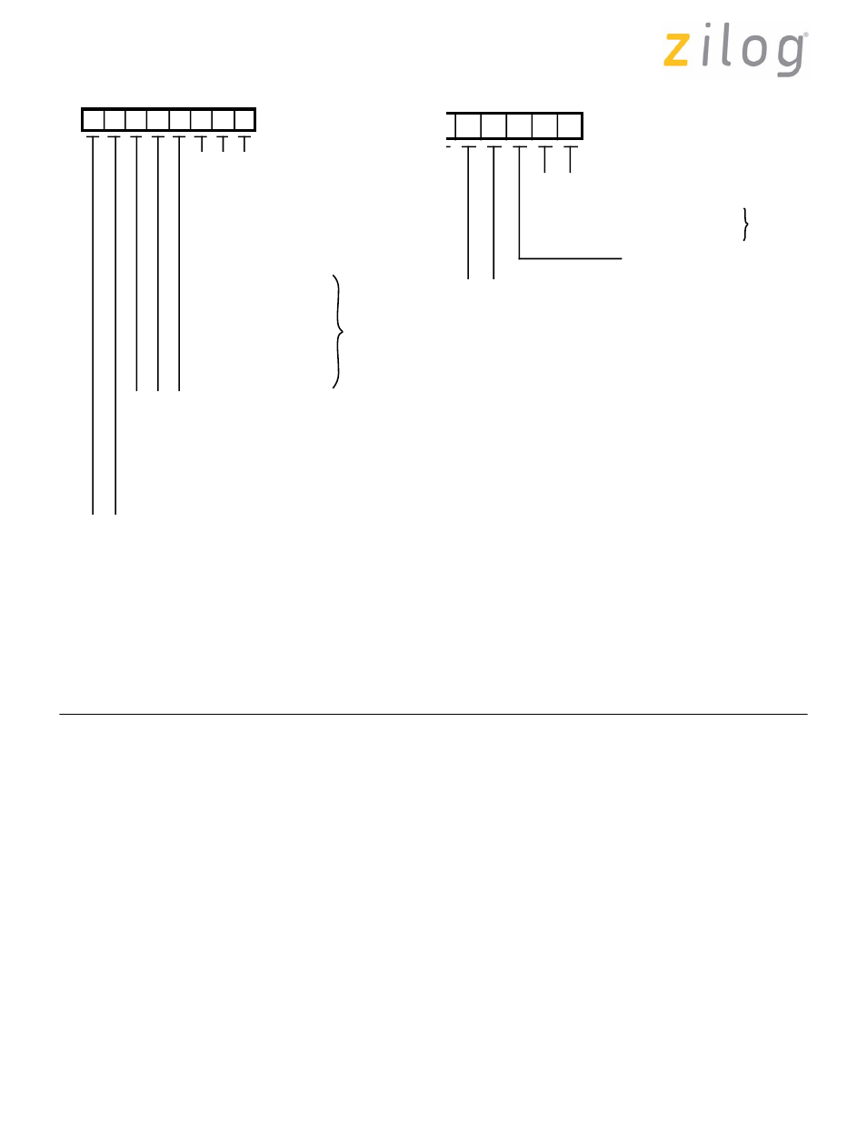
Figure 1. Write Register 0 Bit Functions
(Non-Multiplexed Bus Mode)
Write Register 0 (non-multiplexed bus mode)
D6
D7
D5 D4 D3 D2 D1 D0
Register 0
Register 1
Register 2
Register 3
Register 4
Register 5
Register 6
Register 7
Register 8
Register 9
Register 10
Register 11
Register 12
Register 13
Register 14
Register 15
0
0
1
1
0
0
1
1
0
0
1
1
0
0
1
1
0
1
0
1
0
1
0
1
0
1
0
1
0
1
0
1
0
0
0
0
1
1
1
1
0
0
0
0
1
1
1
1
Null Code
Point High
Reset Ext/Status Interrupts
Send Abort (SDLC)
Enable Int on Next Rx Character
Reset Tx Int Pending
Error Reset
Reset Highest IUS
0
0
1
1
0
0
1
1
0
1
0
1
0
1
0
1
0
0
0
0
1
1
1
1
Null Code
Reset Rx CRC Checker
Reset Tx CRC Generator
Reset Tx Underrun/EOM Latch
0
0
1
1
0
1
0
1
* With Point High Command
*
Figure 2. Write Register 0 Bit Functions
(Multiplexed Bus Mode)
Null Code
Null Code
Select Shift Left Mode
Select Shift Right Mode
Null Code
Null Code
Reset Ext/Status Interrupts
Send Abort
Enable Int on Next Rx Character
Reset Tx Int Pending
Error Reset
Reset Highest IUS
Null Code
Reset Rx CRC Checker
Reset Tx CRC Generator
Reset Tx Underrun/EOM Latch
ster 0 (multiplexed bus mode)
5 D4 D3 D2 D1 D0
0
0
1
1
0
0
1
1
0
1
0
1
0
1
0
1
0
0
1
1
0
1
0
1
0
*
0
0
0
0
nnel Only
Page 307 of 316
UM011002-0808