Zilog Z16C35 User Manual
Page 284

Application Note
Technical Considerations When Implementing LocalTalk Link Access Protocol
14-4
HARDWARE CONFIGURATION
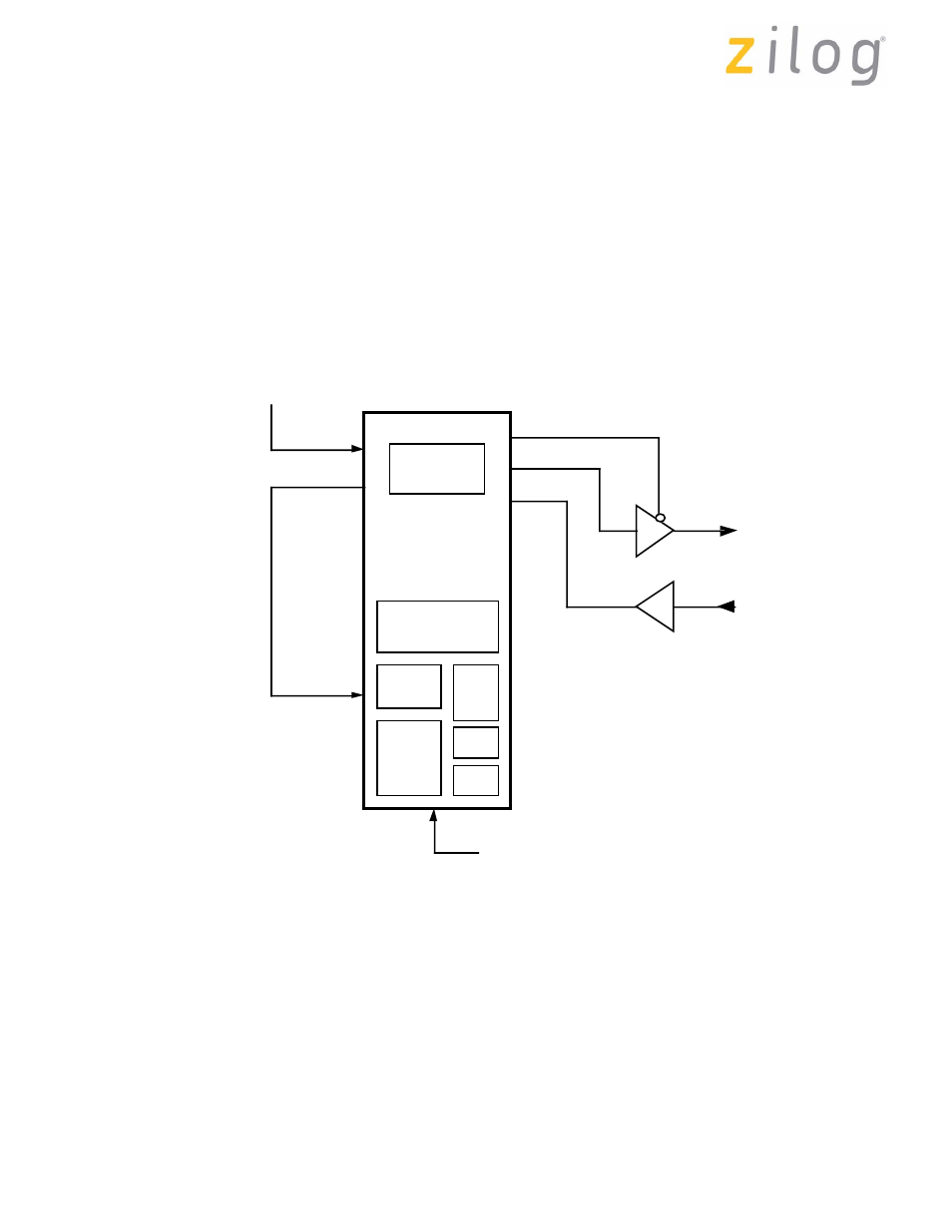
As shown in Figure 2, the hardware used to implement this
LLAP driver consists of the Z80181 (an integration of the
Z80180 compatible MPU core with one channel of a
Z85C30 SCC, Z80 CTC, two 8-bit general-purpose parallel
ports and two chip select signals) operating at 10 MHz, a
3.6864 MHz clock source and an RS-422 line driver with
tri-state.
The SCC’s clocking scheme decouples the micro-
processor’s clock from the communication clock (Figure
3). The DPLL uses the /RTxC pin as its source. The /RTxC
also drives the Baud Rate Generator which divides its
input by sixteen. The resulting 230.4 kHz signal is then
used as transmitter clock. This 230.4 kHz signal is also
used by one of the Z80181’s counter/timer trigger inputs
(Z80 CTC’s channel 1) which is used to count the number
of elapsed bit times. In counter mode, each active edge to
the CTC’s CLK/TRG1 input causes the downcounter of the
CTC to be decremented. The /TRxC pin is programmed as
BRG output and is connected to the CLK/TRG1 input
through an external wire.
The /RTS signal is used to tri-state RS-422 to allow other
node transmitters to drive the line. This signal is asserted
and deasserted through bit1 of the SCC’s Write Register 5.
Figure 2. Driver Hardware Configuration
Addr
Decode
Logic
PIA1
PIA2
SCC/2
CTC
GLU
Z80180
Z80181
3.6864 MHz
/RTxC
CLK/TRIG1
/TRxC
/RTS
TxD
RxD
RS-422 Drivers
To Line
From Line
PCLK = 10 MHz
230.4 kHz
Page 278 of 316
UM011002-0808
