2 general description of the receiver, General description of the receiver, Iscc user manual – Zilog Z16C35 User Manual
Page 53
ISCC
User Manual
UM011002-0808
47
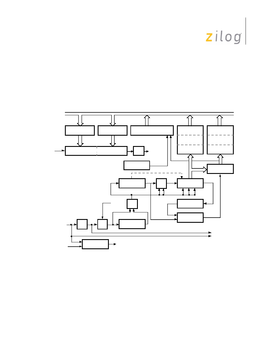
4.1.2 General Description of the Receiver
The receiver has a three deep, 8-bit Data FIFO (paired with a three deep Error FIFO), and
an 8-bit shift register. The receiver block diagram is shown in Figure 4-2. This arrange-
ment creates a three-character delay time, which allows the CPU time to service an inter-
rupt at the beginning of a block of high-speed data. With each Receive Data FIFO, the
Error FIFO stores parity and framing errors and other types of status information. The
Error FIFO is readable in Read Register 1.
Figure 4–17. Receiver Block Diagram
Incoming data is routed through one of several paths depending on the mode and character
length. In Asynchronous mode, serial data enters the 3-bit delay if the character length of
seven or eight bits is selected. If a character length of five or six bits is selected, data enters
the receive shift register directly.
In synchronous modes, the data path is determined by the phase of the receive process cur-
rently in operation. A synchronous receive operation begins with a hunt phase in which a
bit pattern that matches the programmed sync characters (6-,8-, or 16-bit is searched).
WR13 Upper Byte
Time Constant
DPLL
WR12 Lower Byte
Time Constant
10 X 19 Frame
Status FIFO
Internal Data Bus
Receive
Data
FIFO
Receive
Error
FIFO
÷ 2
14-Bit Counter
16-Bit Down Counter
BR
Generator
Output
Receive
Error Logic
Receive Sync
Register (8-Bits)
CRC Delay
Register (8-Bits)
CRC
Checker
3 Bits
Sync Register
& Zero Delete
MUX
Sync
CRC
1-Bit
NRZI Decode
Internal
TxD
DPLL
DPLL Output
MUX
To Transmitter
CRC Result
SDLC CRC
Hunt Mode (Bisync)
BR
Generator
Input
RxD
Page 47 of 316