Zilog Z16C35 User Manual
Page 308
Application Note
On-Chip Oscillator Design
15-8
PRACTICE: CIRCUIT ELEMENT AND LAY OUT CONSIDERATIONS (Continued)
Output Level. The signal at the amplifier output should
swing from ground to V
CC
. This indicates there is adequate
gain in the amplifier. As the oscillator starts up, the signal
amplitude grows until clipping occurs, at which point, the
loop gain is effectively reduced to unity and constant
oscillation is achieved. A signal of less than 2.5 Vp-p is an
indication that low gain may be a problem. Either C1/C2
should be made smaller or a low R crystal should be used.
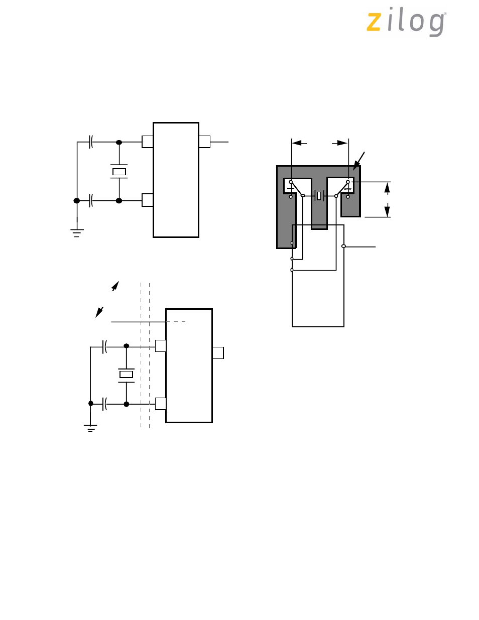
Figure 9. Circuit Board Design Rules
Z80180
Clock Generator Circuit
XTAL
EXTAL
C
2
3
64
L
CL
Z80180
Signal C
Signals A B
2
3
64
(Parallel Traces
Must Be Avoided)
Board Design Example
(Top View)
Z80180
64
CLK
1
20 mm max
20 mm
max
2
3
GND
Signal Line
Layout Should
Avoid High
Lighted Areas
To prevent induced noice, the crystal and load
capacitors should be physically located as
close to the LSI as possible.
Signal lines should not run parallel to the clock
oscillator inputs. In particullar, the clock input
circuitry and the system clock output (pin 64)
should be separated as much as possible.
V power lines should be separated from the
clock oscillator input circuitry.
Resistivity between XTAL or EXTAL and the
other pin should be greater than 10 M
Ω
cc
●
●
●
●
Page 302 of 316
UM011002-0808