Zilog Z16C35 User Manual
Page 152

ISCC
User Manual
UM011002-0808
146
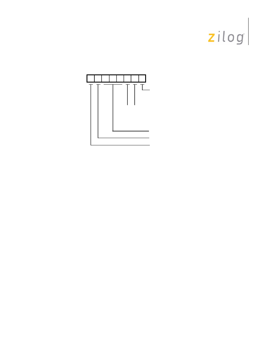
Figure 5–68. Bus Configuration Register
Bit D7 is the Byte Swap Enable
A zero in this bit disables the byte swap feature. Thus the ISCC accepts DMA transferred
data from memory on the lower eight bits of the address data bus (AD) and ignores data on
the upper eight bits.
A one in his bit enables the byte swap feature and the ISCC accepts DMA transferred data
from memory on either the upper or lower eight bits of the bus depending on the state of
A0, the least significant address bit. Big endian or little endian selection is made through
bit D6.
Note that whether or not this feature is enabled, when data is DMA transferred from the
ISCC to memory, the ISCC replicates the same data on both the lower and upper eight bits
of the bus. Writing to memory is controlled by the external generation of appropriate
memory enable or strobe signals.
Bit D6 controls the odd/even byte selection when the Byte Swap feature is enabled. If
Byte Swap Select is a 1, then even address bytes (transfers where the DMA address has
A0 equal to 0) are accepted by the ISCC on the lower eight bits of the bus and odd address
bytes (transfers where the DMA address has A0 equal to 1) are accepted on the upper eight
bits of the bus. If Byte Swap Select is a 0, then even address bytes (transfers where the
DMA address has A0 equal to 0) are accepted by the ISCC on the upper eight bits of the
bus and odd address bytes (transfers where the DMA address has A0 equal to 1) are
accepted on the lower eight bits of the bus.
Bits D5 through D3 are reserved and should be programmed zero.
D6
D7
D5 D4 D3 D2 D1 D0
Shift Right/Left Address
for DMA
Reserved
Byte Swap Select
Byte Swap Enable
Status Acknowledge
Pulsed Acknowledge
Reserved
Double-Pulsed Acknowledge
0
0
1
1
0
1
0
1
Interrupt Acknowledge Type
Page 146 of 316
UM011002-0808
