Zilog Z16C35 User Manual
Page 186
Application Note
The Z180™ Interfaced with the SCC at MHZ
7
7
.
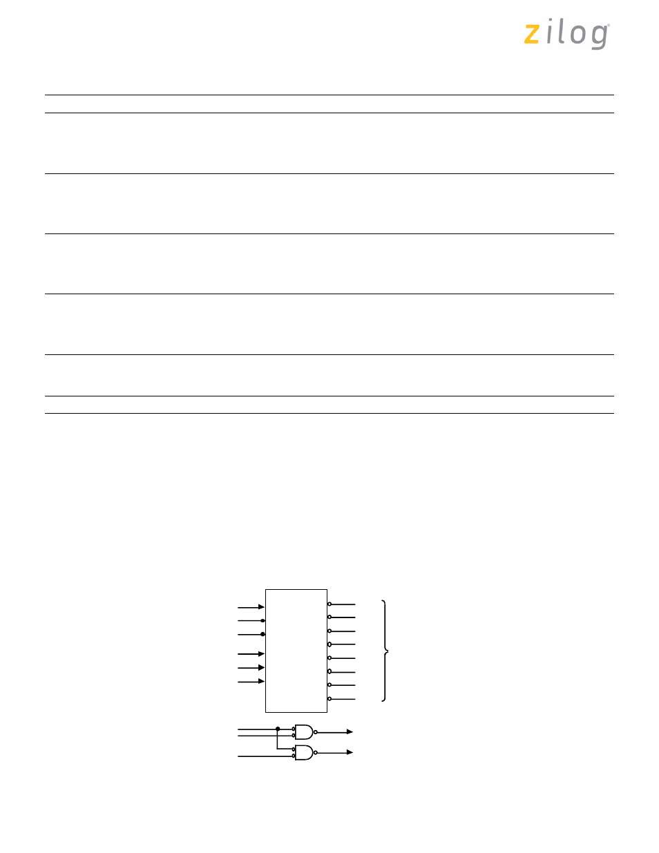
If you are familiar with the Z80 CPU design, the same
interfacing logic applies to the Z180 and I/O interface (see
Figure 9a). This circuit generates /IORD (Read) or IORD
(Write) for peripherals from inputs /IORQ, /RD, and /WR.
The address decodes the Chip Select signal. Note, if you
have Z80 peripherals, the decoder logic decodes only from
addresses (does not have /IORQ). The Z180 signals
/IORQ, /RD, and /WR are active at about the same time
(Parameters #9, 22, 28). However, most of the Z80
peripherals require /CE to /RD or /WR setup time.
Since the Z180 occupies 64 bytes of I/O addressing space
for system control and on-chip peripherals, there are no
overlapping I/O addresses for off-chip peripherals. In this
design, leave the area as default or assign on-chip
registers at I/O address 0000h to 003Fh.
Figure 9 shows a simple address decoder (the required
interface signals, other than address decode outputs, are
discussed later).
Table 5. Z8018010 Timing Parameters for I/O Cycle (Worst Case)
No
Symbol
Parameter
Min
Max
Units
1
tcyc
Clock Cycle Period
100
ns
2
tCHW
Clock Cycle High Width
40
ns
3
tCLW
Clock Cycle Low Width
40
ns
4
tcf
Clock Fall Time
10
ns
6
tAD
Clock High to Address Valid
70
ns
9
tRDD1
Clock High to /RD Low IOC=0
55
ns
11
tAH
Address Hold Time
10
ns
13
tRDD2
Clock Low to /RD High
50
ns
15
tDRS
Data to Clock Setup
25
ns
16
tDRH
Data Read Hold Time
0
ns
21
tWDZ
Clock High to Data Float Delay
60
ns
22
tWRD1
Clock High to /WR Low
50
ns
23
tWDD
Clock Low to Write Data Delay
60
ns
24
tWDS
Write Data Setup to /WR Low
15
ns
25
tWRD2
Clock Low to /WR High
50
ns
26a
tWRP
/WR Pulse Width (I/O Write)
210
ns
27
tWDH
/WR High to Data Hold Time
10
ns
28
tIOD1
Clock High to /IORQ Low IOC=0
55
ns
29
tIOD2
Clock Low to /IORQ High
50
ns
Note:
Parameter numbers in this table are the numbers in the Z180 technical manual.
Figure 9a. I/O Interface Logic (Example)
/G2A
/G2B
C
B
A
A17
A2
A5
A4
A3
/Y9
/Y6
/Y5
/Y4
/Y3
/Y2
/Y1
/Y0
50 ~
58 ~
54 ~
50 ~
40 ~
48 ~
44 ~
40 ~
HCT138
/IORQ
/RD
/WR
/IORD To Each
Peripherals' /RD
/IOWR To Each
Peripherals' /WR
A6
G1
Chip Select Signals
for Peripherals
Page 180 of 316
UM011002-0808