1 architecture -5, Figure 3-1. analog i/o module block diagram -5, 1 architecture – Maxim Integrated MAXQ7666 User Manual
Page 95
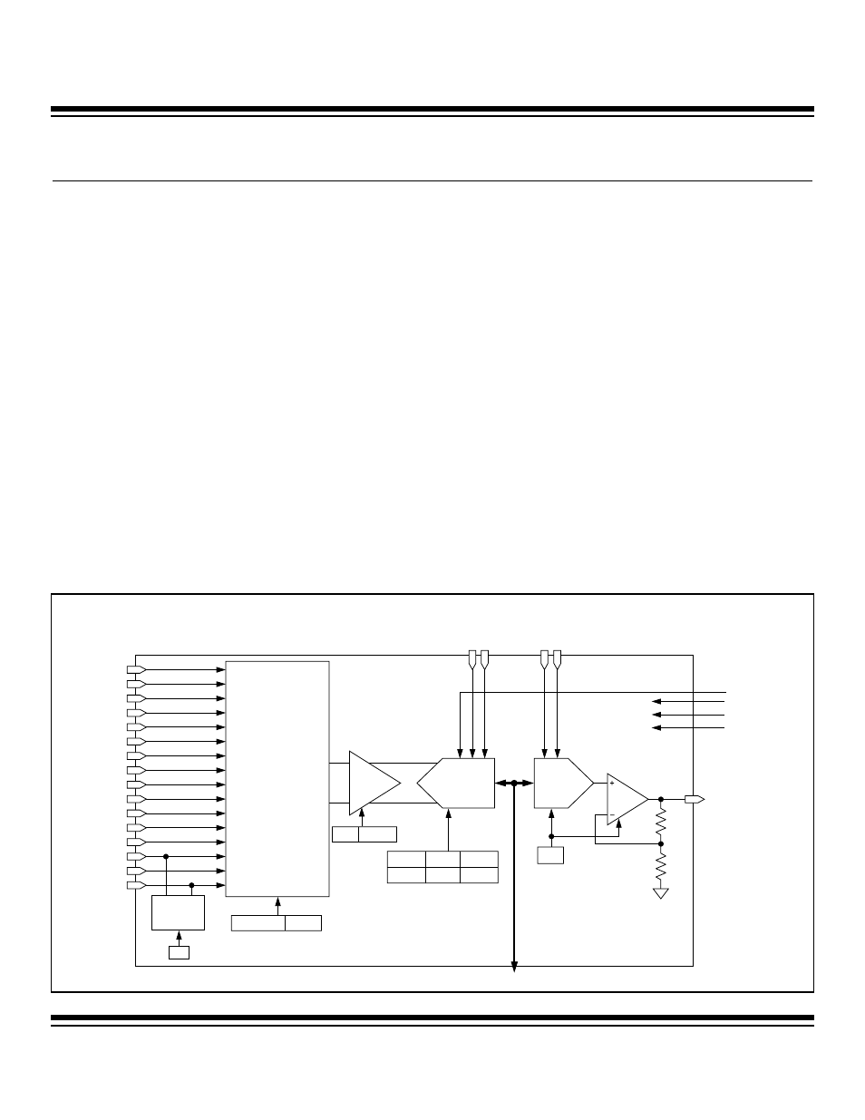
SECTION 3: ANALOG I/O MODULE
The MAXQ7665/MAXQ7666 contain an ultra-low-power precision analog I/O module for measuring and controlling a host of sensors,
motors, bridges, and other analog peripherals. The analog I/O module has all the components to make the MAXQ7665/MAXQ7666
stand-alone data-acquisition machines ideal for harsh environment applications. Except where explicitly noted, the MAXQ7665 and
MAXQ7666 support identical features.
The analog I/O module includes the following features:
• 8 differential analog-input multiplexer
• Low-power, 12-bit, 500ksps successive approximation ADC
• 12-bit, buffered, voltage-output DAC
• On-chip ±1°C accurate temperature sensor (typ)
• Remote temperature sensor drive circuit
• Internal programmable gain amplifier (x1, x2, x4, x8, x16, x32)
• Individual external reference inputs for the ADC and DAC
3.1 Architecture
The analog-input multiplexer supports 8 differential measurements and feeds the programmable gain amplifier (PGA) and the 12-bit
SAR ADC. The low noise, programmable gain amplifier with gains of x1 to x32 allows interfacing to a variety of devices with different
signal amplitudes. The ADC conversion clock source is the same as the system clock source (internal oscillator or external
crystal/clock) and has a user-programmable clock division ratio. The 12-bit voltage-out DAC has internal feedback resistors for reduc-
ing external component count. The internal temperature sensor performs temperature measurements with an internal diode-connect-
ed transistor. In the remote temperature sensor drive configuration, the device provides the proper bias necessary to measure tem-
perature with up to two external diode-connected transistor sensors. The MAXQ7665/MAXQ7666 support independent external refer-
ence inputs for the ADC and DAC to allow the use of high precision, high quality reference sources.
Figure 3-1 shows a functional block diagram of the MAXQ7665/MAXQ7666 analog I/O module.
MAXQ7665/MAXQ7666 User’s Guide
3-5
Figure 3-1. Analog I/O Module Block Diagram
AIN0
AIN1
AIN2
AIN3
AIN4
AIN5
AIN6
AIN7
AIN8
AIN9
AIN10
AIN11
AIN12
AIN13
AIN14
AIN15
PGAE
DACE
12-BIT
500kHz
ADC
12-BIT
DAC
PGA
DATA BUS (15:0)
ANALOG I/O FUNCTIONAL BLOCKS
8 DIFFERENTIAL
CHANNEL
MULTIPLEXER
TIMER 2
TIMER 1
TIMER 0
ADCCLK
VDAC
INTERNAL
TEMP
SENSOR
REFADC
REFDAC
50k
Ω
50k
Ω
TSE
PGG[2:0]
ADCDIF
ADCMX[4:0]
P0.5/
DACLOAD
P0.4/
ADCCNV
ADCS
ADCE
ADCBY ADCDUL
ADCBIP
ADCASD
Maxim Integrated