5 port 0 direction register (pd0) – Maxim Integrated MAXQ7666 User Manual
Page 269
8.2.5 Port 0 Direction Register (PD0)
Register Description:
Port 0 Direction Register
Register Name:
PD0
Register Address:
Module 00h, Index 10h
Bits 15 to 8: Reserved. Read returns 0, write ignored.
Bits 7 to 0: Port 0 Direction Register Bits 7 to 0 (PD0.7 to PD0.0). Port 0 is a Type D I/O port. The PD0 register is used to determine
the direction of each pin that makes up the port. The port pins are independently controlled by their direction bit. When a bit in PD0 is
set to 1, its corresponding pin is enabled as an output. The data value in the respective bit of the PO register will be driven on the pin.
When a bit in PD0 is cleared to 0, its corresponding pin is available as an input, and allows an external signal to drive the pin. Note
that each port pin has a weak pullup resistor when functioning as an input, which is controlled by the respective PO bit. If the PO bit
is set to 1, the pullup is enabled; if the PO bit is cleared to 0, the pullup is disabled and the port pin is in high impedance three-state.
MAXQ7665/MAXQ7666 User’s Guide
8-7
r = read, w = write
Note: This register is cleared to 00h on all forms of reset.
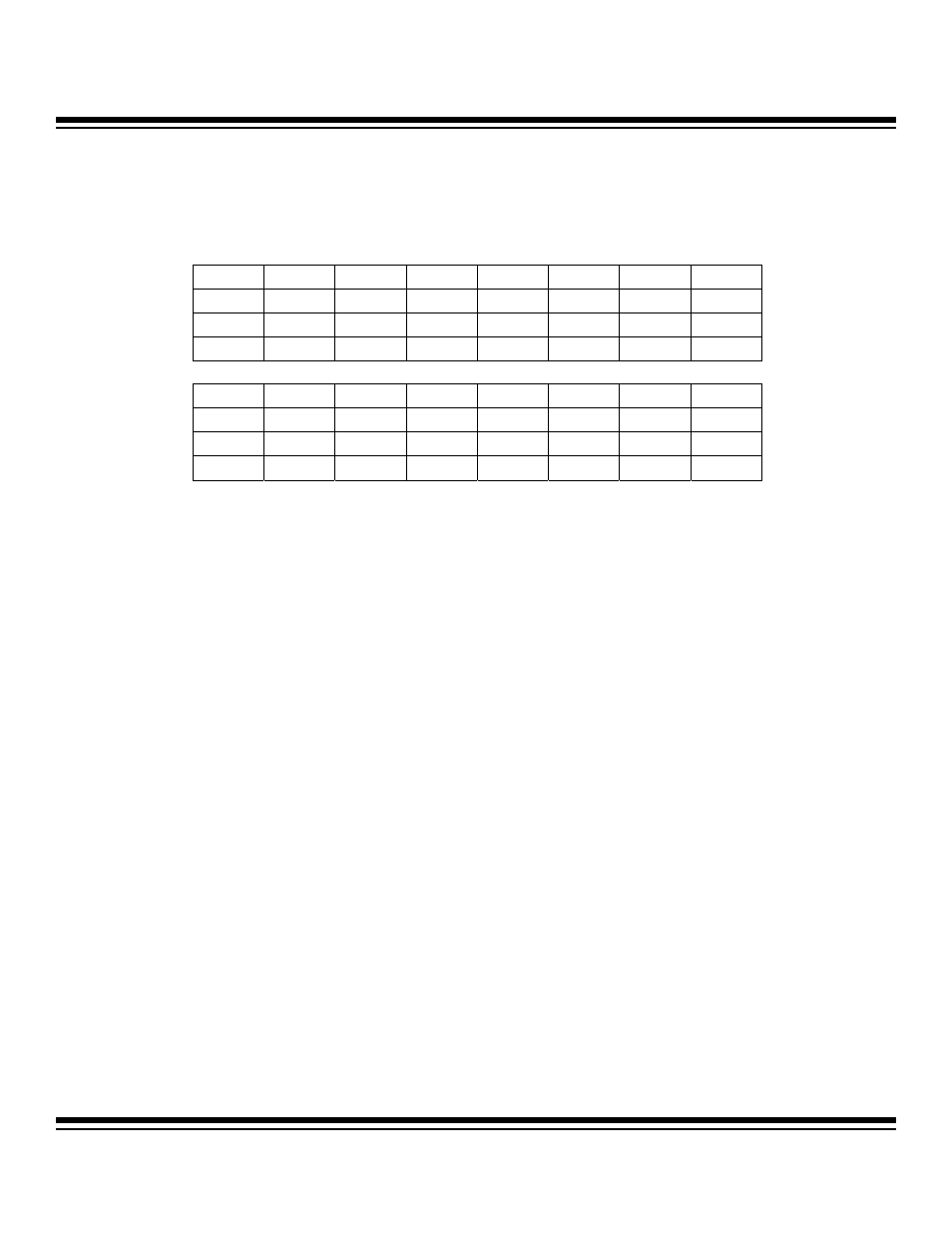
Bit #
15
14
13
12
11
10
9
8
Name
— — — — — — — —
Reset
0 0 0 0 0 0 0 0
Access
r
r
r
r
r
r
r
r
Bit #
7
6
5
4
3
2
1
0
Name
PD0.7 PD0.6 PD0.5 PD0.4 PD0.3 PD0.2 PD0.1 PD0.0
Reset
0 0 0 0 0 0 0 0
Access rw
rw
rw
rw
rw
rw
rw
rw
Maxim Integrated