1 dac signals -38, Figure 3-16. dac block diagram -38, Table 3-12. dac signals -38 – Maxim Integrated MAXQ7666 User Manual
Page 128: Table 3-12. dac signals, 1 dac signals, 2 external reference input and output buffer
MAXQ7665/MAXQ7666 User’s Guide
3-38
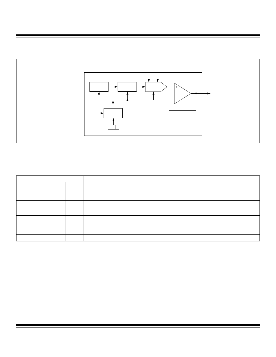
Figure 3-16 shows a simplified functional block diagram of the MAXQ7665/MAXQ7666 DAC.
3.5.1 DAC Signals
The MAXQ7665/MAXQ7666 DAC external signals are explained in Table 3-12.
Table 3-12. DAC Signals
3.5.2 External Reference Input and Output Buffer
The MAXQ7665/MAXQ7666 DAC external reference input, REFDAC, accepts a voltage range extending from 0 to AVDD. The voltage
at REFDAC sets the full-scale output of the DAC. The output voltage is determined using the following equation:
DACOUT = (REFDAC x CODE
12
) / 2
12
Where:
CODE
12
is the numeric value of the DAC’s straight binary input code
DACOUT is the output voltage on the external DACOUT pin
REFDAC is the reference voltage on the external REFDAC pin
The MAXQ7665/MAXQ7666 DAC output-buffer amplifier is unity-gain stable with rail-to-rail output voltage swings.
Figure 3-16. DAC Block Diagram
REFDAC
DACE
DAC OUTPUT
REGISTER
DAC INPUT
REGISTER
DAC LOAD
CONTROL
12-BIT DAC
PO.5/DACLOAD
DACOUT
DACLD
0 1 2
PIN NUMBER
SIGNAL
48-PIN 56-PIN
FUNCTION
REFDAC 7 7
Dedicated DAC Reference Input Pin. The REFDAC pin is used to supply an external precision voltage reference
to the internal DAC. The REFDAC can handle a voltage range from 0 to AV
DD
.
P0.5/DACLOAD 37
43
The DAC load is a shared pin with the digital I/O port 0 bit 5. As the DAC load input signal, it can trigger DAC
conversion by loading the DAC output register on a rising or falling edge. After power-up or a reset this pin
defaults to a digital I/O port pin with pullup enabled.
DACOUT 17 19
Dedicated DAC Output Pin. If the DAC is disabled, this pin is configured as a 100k
pulldown resistor to
ground.
AVDD 44
52
Analog V
DD
Supply. For the MAXQ7665/MAXQ7666, the analog supply voltage is +5.0V.
AGND
5, 8
5, 8
Analog Ground
Maxim Integrated