10 oscillator control register (oscc) -16, 10 oscillator control register (oscc) – Maxim Integrated MAXQ7666 User Manual
Page 106
3.2.10 Oscillator Control Register (OSCC)
Register Description:
Oscillator Control Register
Register Name:
OSCC
Register Address:
Module 05h, Index 0Ch
Bits 15 to 12, 4, and 3: Reserved. Read returns 0, write ignored.
Bits 11 and 10: High-Frequency Crystal Output Capacitance Select 1 and 0 (HFOC1 and HFOC0). See
Section 5 for details on
these bits.
Bits 9 and 8: High-Frequency Crystal Input Capacitance Select 1 and 0 (HFIC1 and HFIC0). See
Section 5 for details on these bits.
Bits 7 to 5: ADC Clock Divider Bits 2 to 0 (ADCCD2 to ADCCD0). These bits determine the ADC clock frequency that is divided
down from the system clock. The MAXQ7665/MAXQ7666 ADC uses the divided-system clock to clock the multiplexer front-end selec-
tion, track and hold acquisition, and each step of the successive approximation conversion. Note that there is no ADC clock in stop
mode.
Bit 2: External High-Frequency Clock Enable (EXTHF). See
Section 5 for details on this bit.
Bit 1: Internal RC Oscillator Enable (RCE). See
Section 5 for details on this bit.
Bit 0: High-Frequency Crystal Oscillator Enable (HFE). See
Section 5 for details on this bit.
MAXQ7665/MAXQ7666 User’s Guide
3-16
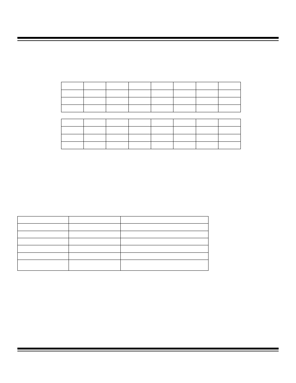
Bit #
15
14
13
12
11
10
9
8
Name
— — — —
HFOC1
HFOC0
HFIC1
HFIC0
Reset
0 0 0 0 0 0 0 0
Access r
r
r
r
rw
rw
rw
rw
Bit #
7
6
5
4
3
2
1
0
Name
ADCCD2 ADCCD1 ADCCD0
—
—
EXTHF
RCE
HFE
Reset
0 0 0 0 0 0 1 0
Access rw
rw
rw
r
r
rw
rw
rw
r = read, w = write (Note that some clock control bits may have locking mechanisms for write.)
Note: This register is cleared to 0002h on power-on reset and is not affected by other forms of reset.
ADCCD2:ADCCD0
DIVIDE RATIO
ADC CLOCK
000
1 (default)
ADC Clock = System Clock
001
2
ADC Clock = System Clock/2
010
4
ADC Clock = System Clock/4
011
8
ADC Clock = System Clock/8
100
16
ADC Clock = System Clock/16
101–111
Reserved,
divide by 16 if set
ADC Clock = System Clock/16
Maxim Integrated