1 oscillator/clock generation module pins -4, 1 oscillator/clock generation module pins – Maxim Integrated MAXQ7666 User Manual
Page 201
5-4
MAXQ7665/MAXQ7666 User’s Guide
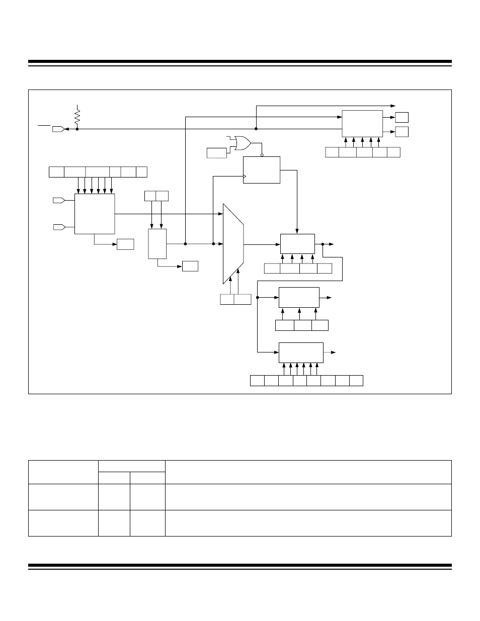
Figure 5-1. Oscillator/Clock Generation Module Block Diagram
POWER-ON RESET
DV
DD
RESET
XIN/
HF-CLK
XOUT
STOP HFIC(1:0)
HIGH-
FREQ
CLOCK/
XTAL
HFOC(1:0)
XT EXTHF HFE
RCE
XHFRY
STOP
RGMD
RC
OSC
STOP
CLOCK
DIVIDE
SYSCLK
EWDI
WDIF
WTRF
WD1
WDT RESET
WATCHDOG
INTERRUPT FLAG
WATCHDOG
TIMER RESET
FLAG
WD0
WATCHDOG
TIMER
EWT
RWT
ADCCLK
SWB
PMME
CD1
ADCD2
BPR6
BPR7
BPR4
BPR5
BPR2 BPR1 BPR0
BPR3
ADCD1 ADCD0
CD0
ADC CLOCK
PRESCALE
CAN CLOCK
PRESCALE
ENABLE
MUX
XT
EXTHF
POWER-
UP TIMER
(/2
16
)
CAN CLOCK
5.1.1 Oscillator/Clock Generation Module Pins
Table 5-1 shows the MAXQ7665/MAXQ7666 oscillator/clock generation module signals.
Table 5-1. MAXQ7665/MAXQ7666 Oscillator/Clock Generation Module Pins
PIN
OSCILLATOR SIGNAL
48
56
DESCRIPTION
XIN 43
49
High-Frequency Crystal Input. Connect an external crystal or resonator between XIN and XOUT as
the high-frequency oscillator clock. Alternatively, XIN is the input for an external high-frequency
clock source when XOUT is floating. Leave XIN unconnected if an external clock source is not used.
XOUT 42
48
High-Frequency Crystal Output. Connect an external crystal or resonator between XIN and XOUT as
the high-frequency oscillator clock. Alternatively, float XOUT when an external, high frequency clock
source is connected to the XIN pin.
Maxim Integrated