1 type 2 status/control registers -7, 1 type 2 status/control registers – Maxim Integrated MAXQ7666 User Manual
Page 242
MAXQ7665/MAXQ7666 User’s Guide
7-7
7.2.1 Type 2 Status/Control Registers
The MAXQ7665/MAXQ7666 timer/counter module registers T2CFGx (configuration), T2CNAx (control A), and T2CNBx (control B),
where x = 0, 1, and 2, are described here.
7.2.1.1 Type 2 Timer/Counter 2 Configuration Register (T2CFGx)
Register Description:
Type 2 Timer/Counter 2 Configuration Register
Register Name:
T2CFGx (x = 0, 1, 2)
Register Address:
T2CFG0: Module 02h, Index 10h
T2CFG1: Module 02h, Index 11h
T2CFG2: Module 03h, Index 10h
Bits 15 to 7: Reserved. Read 0, write ignored.
Bits 6 to 4: Type 2 Timer Clock Divide Bits 2 to 0 (T2DIV2 to T2DIV0). These three bits select the divide ratio for the timer clock
input clock (as a function of the system clock).
Bit 3: Type 2 Timer Mode Select (T2MD). This bit enables the dual 8-bit mode of operation. The default reset state is 0, which selects
the 16-bit mode of operation. When the dual 8-bit mode is established, the primary timer/counter (T2Hx) carries all the counter/cap-
ture functionality, while the secondary 8-bit timer (T2Lx) must operate in timer compare mode, sourcing the defined internal clock.
0 = 16-bit mode (default)
1 = dual 8-bit mode
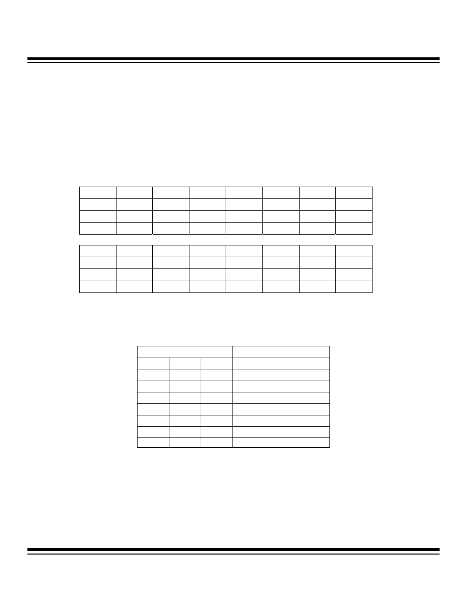
Bit #
15
14
13
12
11
10
9
8
Name — — — — — — — —
Reset 0 0 0 0 0 0 0 0
Access r r r r r r r r
Bit #
7
6
5
4
3
2
1
0
Name
—
T2DIV2 T2DIV1 T2DIV0 T2MD CCF1 CCF0 C/T2
Reset 0 0 0 0 0 0 0 0
Access r rw rw rw rw rw rw rw
T2DIV2:T2DIV0
DIVIDE RATIO
0
0
0
1
0
0
1
2
0
1
0
4
0
1
1
8
1
0
0
16
1
0
1
32
1
1
0
64
1
1
1
128
r = read, w = write
Maxim Integrated