27 data pointer 1 register (dp[1]) -61, 5 peripheral register modules -61, 5 peripheral register modules – Maxim Integrated MAXQ7666 User Manual
Page 63: 27 data pointer 1 register (dp[1])
1.4.27 Data Pointer 1 Register (DP[1])
Register Description:
Data Pointer 1 Register
Register Name:
DP[1]
Register Address:
Module 0Fh, Index 07h
Bits 15 to 0: Data Pointer 1 Register Bits 15 to 0 (DP[1].15 to DP[1].0). This register is used as a pointer to access data memory.
DP[1] can be automatically incremented or decremented following each read operation or can be automatically incremented or decre-
mented before each write operation.
1.5 Peripheral Register Modules
The MAXQ7665/MAXQ7666 microcontrollers use peripheral registers to control and monitor peripheral modules. These registers reside
in Modules 0h to 5h, with subindex values 0h to 1Fh. The MAXQ7665/MAXQ7666 peripheral register map is shown in Table 1-10. The
peripheral register module bit function and reset values are shown in Table 1-11. Each peripheral module and its associated regis-
ters/bits are covered separately in the following sections.
MAXQ7665/MAXQ7666 User’s Guide
1-61
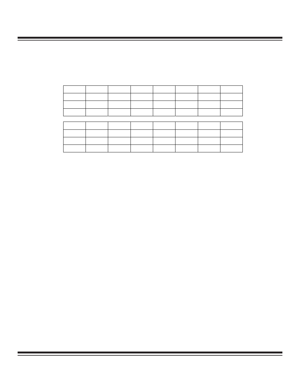
Bit #
15
14
13
12
11
10
9
8
Name
DP[1].15 DP[1].14 DP[1].13 DP[1].12 DP[1].11 DP[1].10 DP[1].9 DP[1].8
Reset
0 0 0 0 0 0 0 0
Access rw
rw
rw
rw
rw
rw
rw
rw
Bit #
7
6
5
4
3
2
1
0
Name
DP[1].7 DP[1].6 DP[1].5 DP[1].4 DP[1].3 DP[1].2 DP[1].1 DP[1].0
Reset
0 0 0 0 0 0 0 0
Access rw
rw
rw
rw
rw
rw
rw
rw
r = read, w = write
Note: This register is cleared to 0000h on all forms of reset.
Maxim Integrated