7 analog input protection -26, 7 analog input protection – Maxim Integrated MAXQ7666 User Manual
Page 116
MAXQ7665/MAXQ7666 User’s Guide
3-26
3.3.7 Analog Input Protection
Internal ESD protection diodes limit all analog inputs to AVDD and AGND, allowing the inputs to swing from (AGND - 0.3V) to (AVDD
+ 0.3V) without damage. However, for accurate conversions near full scale, the inputs should not exceed AVDD by more than +50mV
or be lower than AGND by -50mV. Input voltages beyond AGND - 0.3V and AVDD + 0.3V forward bias the internal protection diodes.
In this situation, limit the forward diode current to 50mA to avoid damaging the MAXQ7665/MAXQ7666.
The MAXQ7665/MAXQ7666’s common-mode analog input range or absolute analog input range is specified from AGND to AVDD.
Signals may run outside that range but will be interpreted as an overrange (ADC data output set to 0xFFF in unipolar mode and to
0x7FF in bipolar mode) or an underrange condition (ADC data output set to 0x000 in unipolar mode and to 0x800 in bipolar mode).
Analog input signals cannot excurse outside of the ABS max input signal ratings of +0.3V above AVDD or -0.3V below AGND.
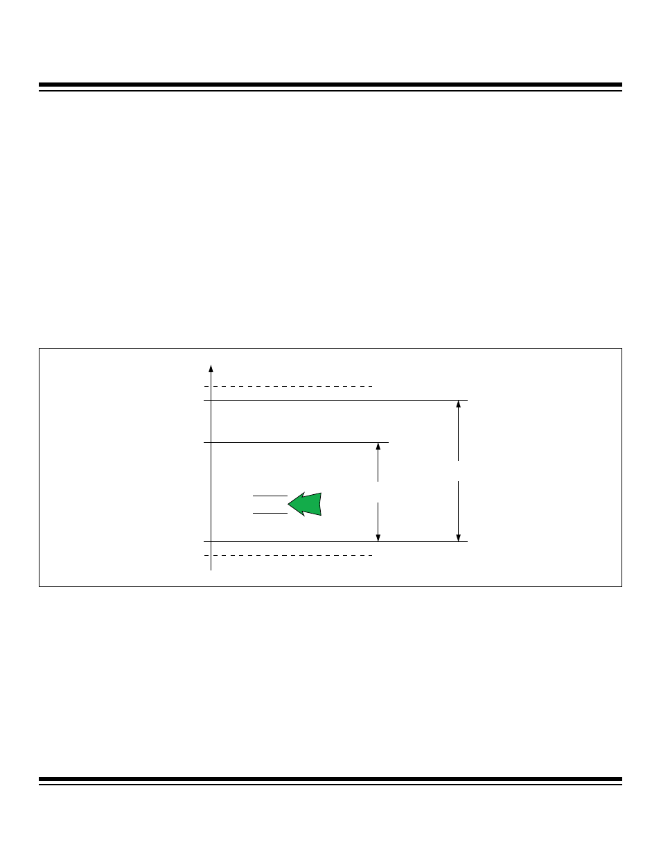
Figure 3-8 shows the common mode or absolute analog input range as specified with a selected REFADC value. In unipolar input con-
figuration (ADCBIP = 0, register bit location ACNT.9), the output data coding of the ADC is straight binary.
In bipolar input configuration (ADCBIP = 1, register bit location ACNT.9), the output data coding of the ADC is two’s complement.
Bipolar mode is commonly used with a differential analog input configuration (ADCDIF = 1, register bit location ACNT.10), where the
analog input signals are referenced to their complementary analog input (AIN+/-) pin. Figure 3-9 shows how a negative ADC value is
created. The absolute voltage of each analog input signal must be within the MAXQ7665/MAXQ7666 supply range so as to satisfy the
critical absolute maximum tolerance ratings of the analog inputs, and must also be within the REFADC range to produce useful infor-
mation from the ADC.
Figure 3-8. Analog Input Range Measuring a Positive Analog Input Value
REFADC
REFADC MAX INPUT = AVDD
AGND
AGND - 0.3V
AVDD
AVDD + 0.3V
ABS MAX+
ABS MAX-
AIN+
AIN-
ADCIN = (AIN+ - AIN-) x PGA GAIN
REFADC MIN INPUT = 1V
DIFFERENTIAL
ANALOG
INPUT
DIFFERENTIAL INPUT
VOLTAGE RANGE
ABSOLUTE INPUT RANGE
(EITHER AIN+ OR AIN- PIN)
Maxim Integrated