2 external reference input and output buffer -38, 3 loading dac data register for conversion -39, Table 3-14. dac load control selection -39 – Maxim Integrated MAXQ7666 User Manual
Page 129: Table 3-14. dac load control selection, 3 loading dac data register for conversion
MAXQ7665/MAXQ7666 User’s Guide
3-39
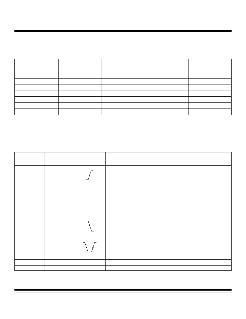
Table 3-13 illustrates the relationship between the straight binary input and the analog output voltage.
Table 3-13. DAC Input Code to Output Voltage (Gain = 1)
3.5.3 Loading DAC Data Register for Conversion
The MAXQ7665/MAXQ7666 DAC conversion is controlled by the DACLD bits in the DAC control register (DCNT). DACLD selects when
and from where the conversion data is sourced. The DAC conversion data is normally sourced from the 12-bit DAC output register
(DACO) except in square-wave mode when the 12-bit DAC input register also acts as a source. The DAC output signal (DACOUT) then
immediately tracks the conversion data source value. The DACLD bits functionality is explained in Table 3-14.
Table 3-14. DAC Load Control Selection
*
Note that as the DAC settling time is up to 15µs, toggling DACLOAD at rates substantially faster than that may not allow to settle at either of the intended out-
put values.
BINARY DIGITAL
INPUT CODE
D11:D0
HEXADECIMAL
EQUIVALENT OF D11:D0
DECIMAL EQUIVALENT
OF D11:D0 (CODE12)
NOMINAL OUTPUT
ANALOG VOLTAGE (V)
NOMINAL OUTPUT
VOLTAGE (V)
(REFDAC = 4.096V)
1111 1111 1111
0xFFF
4095
REFDAC x (4095/4096)
+4.095
1111 1111 1110
0xFFE
4094
REFDAC x (4094/4096)
+4.094
1000 0000 0001
0x801
2049
REFDAC x (2049/4096)
+2.049
1000 0000 0000
0x800
2048
REFDAC x (2048/4096)
+2.048
0111 1111 1111
0x7FF
2047
REFDAC x (2047/4096)
+2.047
0000 0000 0001
0x001
1
REFDAC x (1/4096)
+0.001
0000 0000 0000
0x000
0
0
+0.000
DACLD2:DACLD0
DAC
CONVERSION
SOURCE
DAC CONVERSION
TRIGGER
DAC DATA TRANSFER AND CONTROL
000 DACO
Register
DAC conversion data is sourced from DACO register under the control of the external
DACLOAD input signal. On the rising edge of the DACLOAD input, the DACO register
is loaded with the contents of DACI register and converted. The DAC output signal
(DACOUT) then immediately tracks the DACO value. Note that this selection enables
DACLOAD alternate function on the shared P0.5/DACLOAD pin.
001 DACO
Register
Load conversion
data to DACI
DAC conversion data is sourced from DACO register under the control of software
write to DACI register. The DACO register is loaded with the new contents of DACI
when the DACI register is written. The DAC output signal (DACOUT) then
immediately tracks the DACO value.
010 — —
Reserved
011
—
—
Reserved, functions as 001 if set.
100 DACO
Register
DAC conversion data is sourced from DACO register under the control of the external
DACLOAD input signal. On the falling edge of the DACLOAD input, the DACO
register is loaded with the contents of DACI register and converted. The DAC output
signal (DACOUT) then immediately tracks the DACO value. Note that this selection
enables DACLOAD alternate function on the shared P0.5/DACLOAD pin.
101
DACI and DACO
Registers
Square-Wave Mode. The data source for conversion is dependent upon edges
supplied by the DACLOAD input signal. A falling edge on DACLOAD after entering
square-wave mode will supply the data in DACI to the DAC. A rising edge on
DACLOAD after entering square-wave mode will supply the data in DACO to the
DAC. The DAC output signal (DACOUT) tracks the DACI value on a falling edge and
the DACO value on a rising edge.*
110
—
—
Reserved, functions as 000 if set.
111
—
—
Reserved, functions as 000 if set
Maxim Integrated