2 hardware multiplier peripheral registers -3, 1 hardware multiplier control register (mcnt) -3, 2 hardware multiplier peripheral registers – Maxim Integrated MAXQ7666 User Manual
Page 330: 1 hardware multiplier control register (mcnt)
13.2 Hardware Multiplier Peripheral Registers
13.2.1 Hardware Multiplier Control Register (MCNT)
Register Description:
Hardware Multiplier Control Register
Register Name:
MCNT
Register Address:
Module 001, Index 00h
Bits 15 to 8: Reserved. Read returns 0, write ignored.
Bit 7: Overflow Flag (OF). This bit is set to logic 1 when an overflow occurred for the last operation. This bit can be set for accumu-
lation/subtraction operations or unsigned multiply-negate attempts. This bit is automatically cleared to 0 following a reset, starting a
multiplier operation, or setting of the CLD bit to 0.
Bit 6: MC Register Write Select (MCW). The state of the MCW bit determines if an operation result will be placed into the accumula-
tor registers (MC).
0 = The result is written to the MC registers.
1 = The result is not written to the MC registers (MC register content is unchanged).
Bit 5: Clear Data Registers (CLD). This bit initializes the operand registers and the accumulator of the multiplier. When it is set to 1,
the contents of all data registers and the OF bit are cleared to 0 and the operand load counter is reset immediately. This bit is cleared
by hardware automatically. Writing a 0 to this bit has no effect.
Bit 4: Square Function Enable (SQU). This bit supports the hardware square function. When this bit is set to logic 1, a square oper-
ation is initiated after an operand is written to either the MA or the MB register. Writing data to either of the operand registers writes to
both registers and triggers the specified square or square-accumulate/subtract operation. Setting this bit to 1 also overrides the OPCS
bit setting. When SQU is cleared to logic 0, the hardware square function is disabled.
0 = Square function disabled.
1 = Square function enabled.
MAXQ7665/MAXQ7666 User’s Guide
13-3
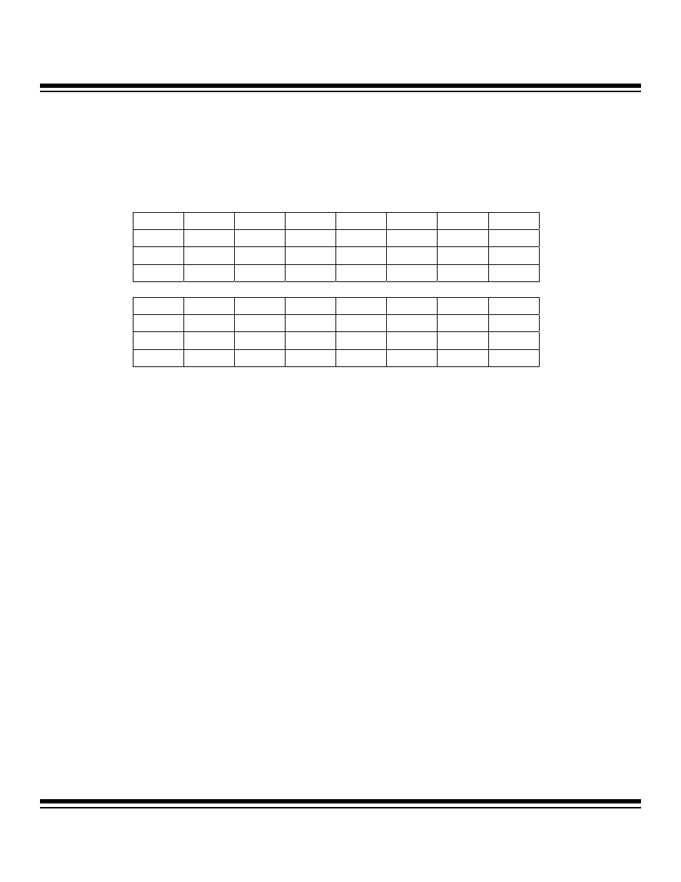
Bit #
15
14
13
12
11
10
9
8
Name
—
—
—
—
—
—
—
—
Reset
0 0 0 0 0 0 0 0
Access
r
r
r
r
r
r
r
r
Bit #
7
6
5
4
3
2
1
0
Name OF
MCW
CLD
SQU
OPCS
MSUB
MMAC
SUS
Reset
0 0 0 0 0 0 0 0
Access r
rw
rw
rw
rw
rw
rw
rw
r = read, w = write
Note: This register is cleared to 0000h on all forms of reset.
Maxim Integrated