1 adc signals -18, 2 differential inputs -18, Table 3-2. adc signals -18 – Maxim Integrated MAXQ7666 User Manual
Page 108: Table 3-2. adc signals, 1 adc signals, 2 differential inputs
MAXQ7665/MAXQ7666 User’s Guide
3-18
3.3.1 ADC Signals
The MAXQ7665/MAXQ7666 ADC uses 18 external signals (other than analog supply and ground) as explained in Table 3-2.
Table 3-2. ADC Signals
3.3.2 Differential Inputs
The MAXQ7665/MAXQ7666 ADC use a fully differential successive-approximation register (SAR) conversion technique and an on-chip
T/H block to convert temperature and voltage signals into a 12-bit digital result. Differential configurations are supported using an ana-
log input channel multiplexer that supports 8 differential channels.
In differential input configuration, analog inputs AIN+ and AIN- are selected from the following pairs: AIN0/AIN1, AIN2/AIN3, AIN4/AIN5,
AIN6/AIN7, AIN8/AIN9, AIN10/AIN11, AIN12/AIN13, and AIN14/AIN15. The differential input configuration references all input signals
to the complementary multiplexer channel input, minimizing common-mode DC offsets and noise. Figure 3-3 shows the multiplexer
connection scheme. The analog input is configured for differential conversion by writing logic 1 to the ADCDIF control bit, while ana-
log input channel selection is controlled by the ADCMX control field in the ACNT peripheral register.
The remote temperature sensor configuration in differential mode uses analog input channel pairs AIN2/AIN3 and/or AIN0/AIN1. In sin-
gle-ended remote temperature sensor configuration, only channels AIN2 and AIN0 are used. Internal temperature sensor configura-
tion measures local die temperature and does not use any analog input channel.
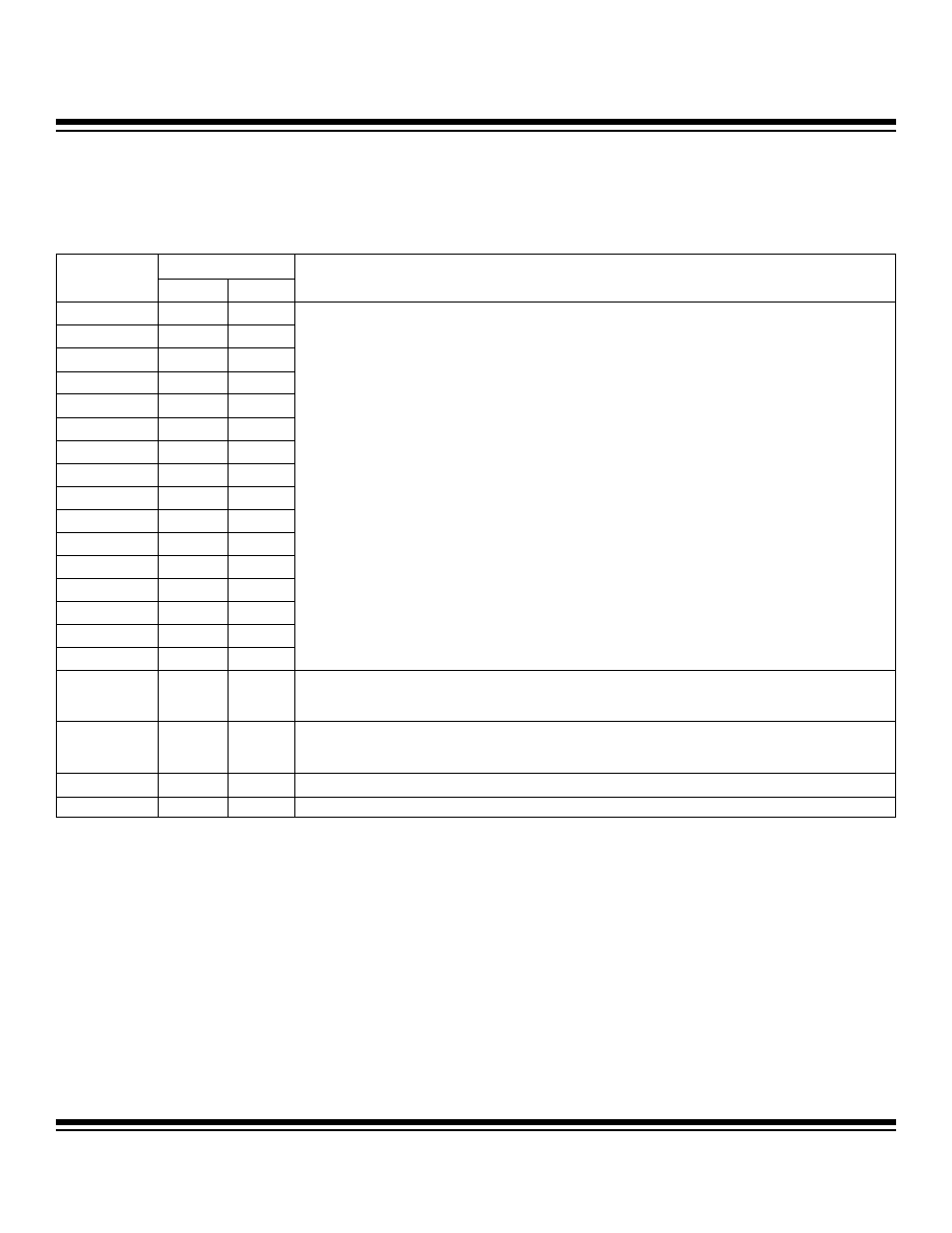
PIN NUMBER
SIGNAL
48-PIN 56-PIN
FUNCTION
AIN15 45
53
AIN14 46
54
AIN13 47
55
AIN12 48
56
AIN11 1 1
AIN10 2 2
AIN9 3
3
AIN8 4
4
AIN7 9
11
AIN6 10
12
AIN5 11
13
AIN4 12
14
AIN3 13
15
AIN2 14
16
AIN1 15
17
AIN0 16
18
ADC Analog Input 15 to 0. These are dedicated analog input pins connected through the internal analog
multiplexer to the PGA and ADC. The analog multiplexer supports 8 differential-input measurements. In
differential input mode, the inputs are paired: AIN14 to AIN15, AIN12 to AIN13, AIN10 to AIN11, AIN8 to
AIN9, AIN6 to AIN7, AIN4 to AIN5, AIN2 to AIN3, AIN0 to AIN1.
(See Section 3.4: Temperature Sensor for discussion on using analog inputs AIN2 and AIN0 for measuring
remote temperature.)
P0.4/ADCCNV 36
41
Port 0 Data Bit 4/ADC Conversion Start. The ADC conversion start is a shared pin with the digital I/O port 0
bit 4. As ADCCNV, this pin can trigger ADC sampling and conversion on a rising or falling edge. After
power-up or a reset this pin defaults to a digital I/O port pin with pullup enabled.
REFADC 6 6
ADC Reference Input. The REFADC input pin is used to supply an external precision voltage reference to
the ADC. The REFADC can handle a voltage range from 1V to AVDD. The REFADC input determines the
full-scale range (FSR) of the internal 12-bit ADC.
AVDD 44
52
Analog V
DD
Supply. For the MAXQ7665/MAXQ7666, the analog supply voltage is +5.0V.
AGND
5, 8
5, 8
Analog Ground
Maxim Integrated