3 system clock control register (ckcn) -8, 3 system clock control register (ckcn) – Maxim Integrated MAXQ7666 User Manual
Page 205
5.2.3 System Clock Control Register (CKCN)
The 8-bit CKCN register is part of the system register group and used to support system clock generation. It controls the system clock
speed and power management mode selection.
Register Description:
System Clock Control Register
Register Name:
CKCN
Register Address:
Module 08h, Index 0Eh
Bit 7: External Crystal Select (XT). This bit selects the external crystal/clock or the internal 7.6MHz RC oscillator as the desired clock
source. The XT bit is the inverse of RGMD except during the crystal warmup period when resuming from the stop mode through the
7.6MHz RC oscillator. This bit is cleared to 0 after a power-on reset, which selects the internal 7.6MHz RC oscillator as the clock source;
otherwise, it is unchanged by other forms of reset.
Changing the XT bit from 0 to 1 causes the system clock source to swap from the internal RC to the high-frequency crystal oscillator.
This change occurs automatically within a few clock cycles if sufficient crystal warmup time has elapsed since the HFE bit of the OSCC
register was set. If the crystal has not finished warming up when XT is set to 1, the crystal oscillator continues to warm up and the clock
source swaps to crystal when this is complete. The XHFRY bit of the ASR register indicates when the crystal oscillator circuit is ready
and the clock source can swap from 7.6MHz RC oscillator to crystal.
Changing the XT bit from 1 to 0 selects the internal 7.6MHz RC oscillator as the system clock source. Allow four 7.6MHz RC oscillator
cycles after enabling the 7.6MHz RC oscillator (RCE = 1) before switching XT to 0. To use the 7.6MHz RC oscillator, the RCE bit in the
OSCC register must be set to logic 1, which enables the 7.6MHz RC oscillator.
Bit 6: Reserved. Read 0, write ignored.
Bit 5: 7.6MHz RC Oscillator Mode (RGMD). This read-only bit reflects the selection of clock source. RGMD = 1 indicates that the
7.6MHz RC oscillator is providing the system clock. RGMD = 0 indicates that the external crystal/clock is providing the system clock.
Note that RGMD is set to 1 only for POR reset.
Bit 4: Stop Mode Select (STOP). Setting this bit to 1 causes the MAXQ7665/MAXQ7666 to enter stop mode. This will not change the
currently selected clock divide ratio (CD0, CD1, and PMME). This bit is cleared by a reset or any of the enabled external interrupts.
Stop mode disables all circuits within the MAXQ7665/MAXQ7666 including the watchdog timer and its clock source (the internal
7.6MHz RC oscillator). All clock sources, timers, and peripherals are halted, and no code execution occurs. The system clock is
stopped, and all processing activity is halted.
Bit 3: Switchback Enable (SWB). If the SWB bit is cleared to 0, switchback mode is not active. If the SWB is set to 1, switchback
mode is active. Switchback mode has no effect if power management mode is not active (PMME = 0). If power management mode is
active and switchback mode is enabled, the PMME bit will be cleared to 0 when any of the following conditions occur:
• An external interrupt condition occurs on a port pin and the corresponding external interrupt is enabled.
• An active-low transition occurs on the UART serial receive-input line (modes 1, 2, and 3) and data reception is enabled.
• The SBUF0 register is written to send an outgoing byte through the UART and transmission is enabled.
• The SPIB register is written in master mode (STBY = 1) to send an outgoing character through the SPI module and transmis-
sion is enabled.
MAXQ7665/MAXQ7666 User’s Guide
5-8
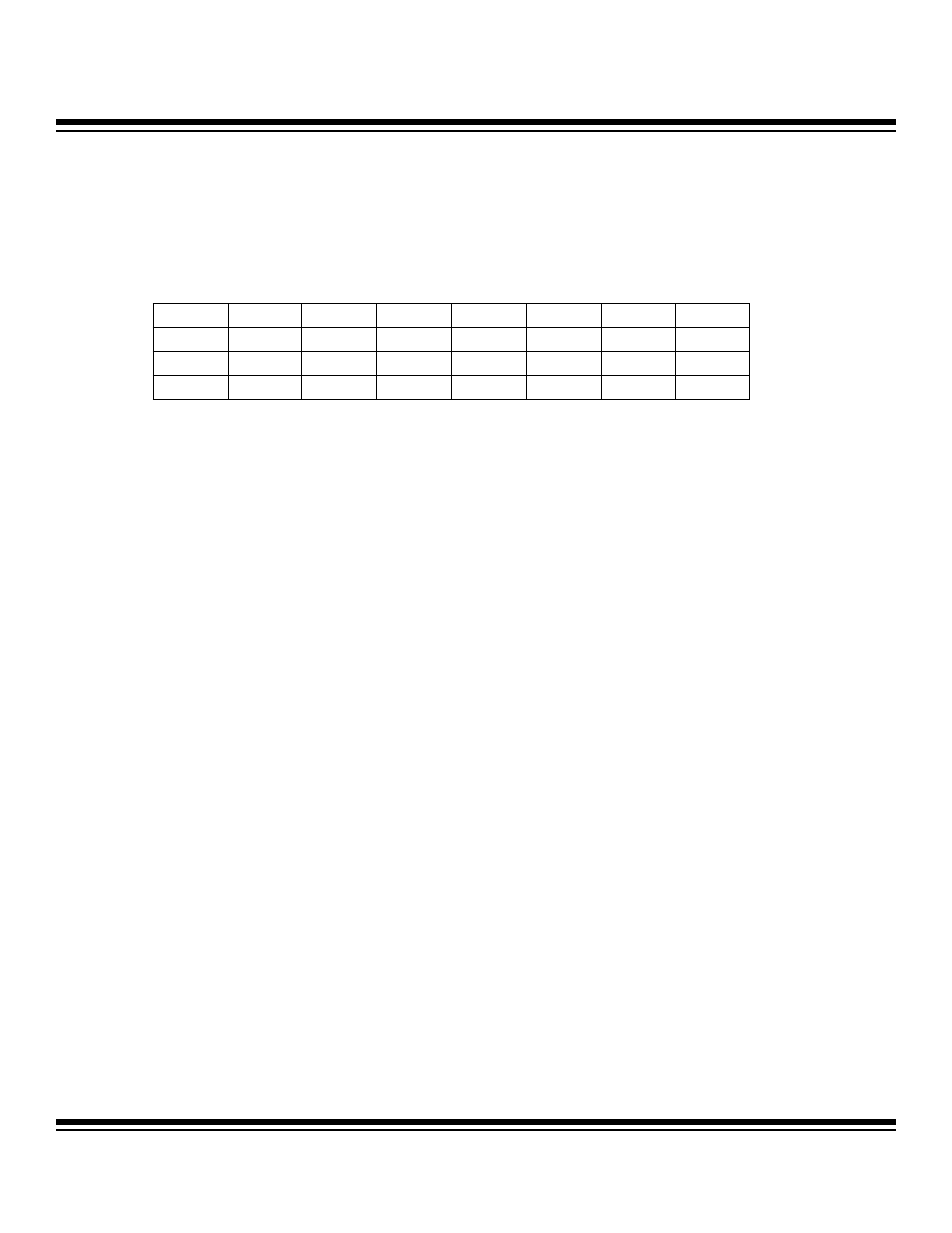
Bit #
7
6
5
4
3
2
1
0
Name XT
—
RGMD
STOP
SWB
PMME
CD1
CD0
Reset 0 0 1 0 0 0 0 1
Access rw r
r
rw
rw
rw
rw
rw
r = read, w = write
Note: Bits 4:0 are set to 00001b on all forms of reset. See bit description for bits 7 and 5.
Maxim Integrated