3 external clock (direct input) -16, 4 internal system clock generation -16, Table 5-3. system clock rate control settings -16 – Maxim Integrated MAXQ7666 User Manual
Page 213: Table 5-3. system clock rate control settings, 3 external clock (direct input), 4 internal system clock generation
MAXQ7665/MAXQ7666 User’s Guide
5-16
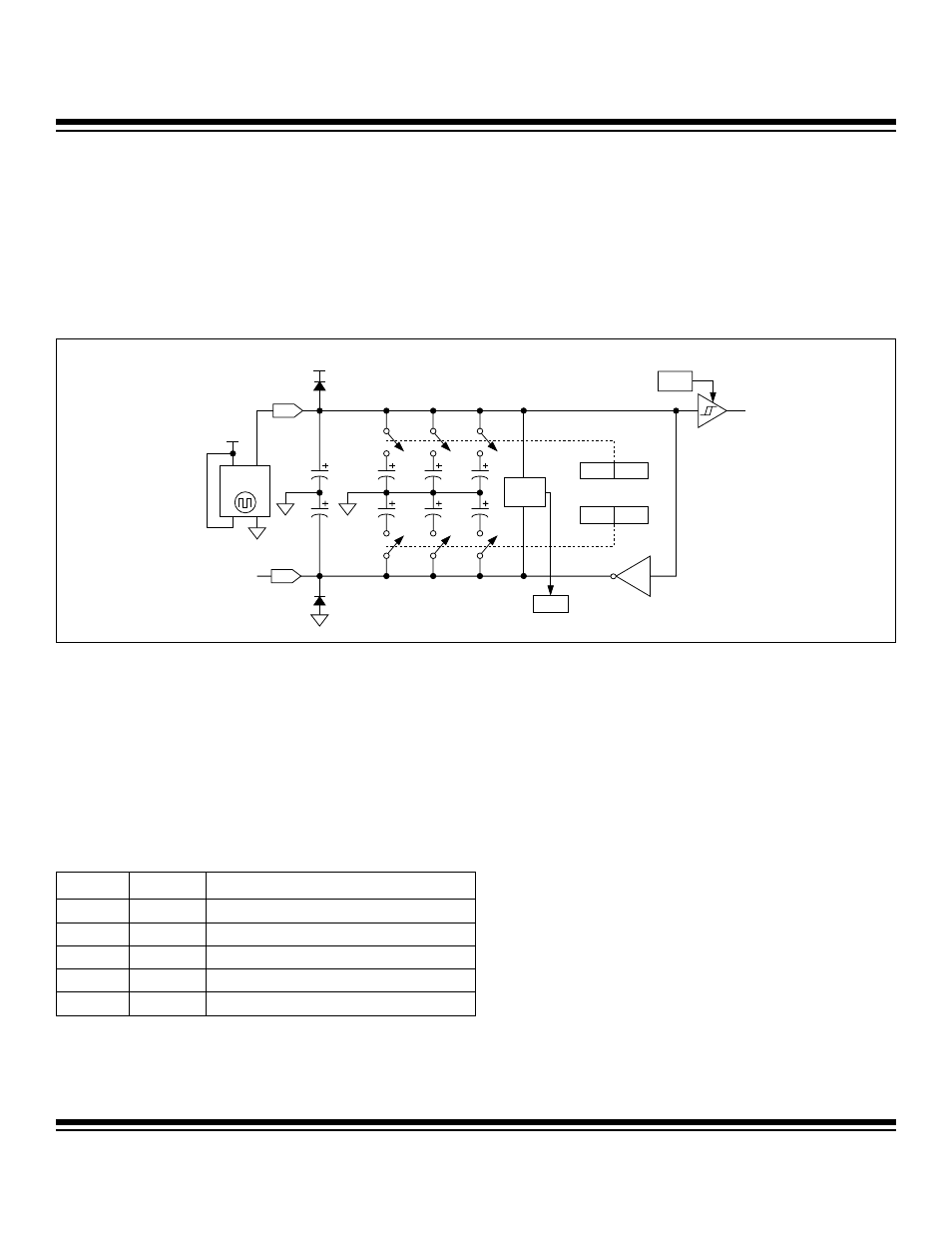
5.3.3 External Clock (Direct Input)
The MAXQ7665/MAXQ7666 can also obtain the system clock signal directly from an external source. In this configuration, the clock
generation circuitry is driven directly by an external clock.
To operate from an external clock, connect the clock source to the XIN pin and leave the XOUT pin floating. Figure 5-6 shows the exter-
nal clock source configuration. The clock source should be driven through a CMOS driver at the same level as DVDD (nominally +3.3V).
If the clock driver is a TTL gate, its output must be connected to DVDD through a pullup resistor to ensure a satisfactory logic level for
active clock pulses. The MAXQ7665/MAXQ7666 are designed to operate at a maximum frequency of 8MHz. For more details, refer to
the MAXQ7665/MAXQ7666 data sheet.
The external clock input is disabled upon power-up, as the default mode for the MAXQ7665/MAXQ7666 is to run from the internal
7.6MHz RC oscillator. To use the external clock input, the EXTHF bit (OSCC.2) must be set to 1. To select the external clock as the sys-
tem clock source, the XT bit (CKCN.7) must be set to 1. When the external clock input is used as the system clock source, the clock
is divided down according to the PMME, CD1, CD0 bit selections (CKCN.2:CKCN.0).
5.3.4 Internal System Clock Generation
The internal system clock is derived from the currently selected system clock source. By default, two system clock cycles are gener-
ated per oscillator clock source cycle, but the number of oscillator clock cycles per system clock can also be increased by setting the
power management mode enable (PMME) bit and the clock-divide control (CD1:CD0) bits per Table 5-3.
Table 5-3. System Clock Rate Control Settings
11pF
STOP
AGC
11pF
7pF
6pF
OSC
0–8MHz
9pF
9pF
7pF
7pF
FAIL
DETECT
HFCI1 HFCI0
HFCO1 HFCO0
XOUT
XIN
DV
DD
DV
DD
HFFINT
Figure 5-6. External Clock Source Configuration
PMME
CD[1:0]
CYCLES PER SOURCE CLOCK
0 00
1
0 01
2
(default)
0 10
4
0 11
8
1 00
256
Maxim Integrated