6 programmable gain amplifier -25, Figure 3-7. pga block diagram -25, 6 programmable gain amplifier – Maxim Integrated MAXQ7666 User Manual
Page 115
MAXQ7665/MAXQ7666 User’s Guide
3-25
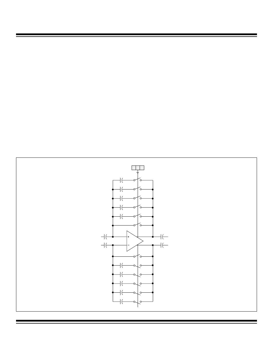
3.3.6 Programmable Gain Amplifier
The MAXQ7665/MAXQ7666 programmable gain amplifier (PGA) receives its inputs from the input multiplexer and feeds its outputs to the
12-bit ADC. Figure 3-7 shows the MAXQ7665/MAXQ7666 PGA block diagram. The PGA has software-selectable gains of x1, x2, x4, x8,
x16, and x32. The PGA uses a switched capacitor technique that reduces power and improves linearity and accuracy. The PGA has a 5µs
warmup/turn-on time from the PGA enable (bit 3 in APE register). The analog front-end should be configured before attempting any con-
versions to ensure that the PGA and ADC are enabled and fully functional. This is most important after a power-down or reset condition.
The MAXQ7665/MAXQ7666 PGA is bypassed when set to gain = 1 (PGG2:PGG0 = 000). If the PGAE bit in the APE register is cleared
(PGA disabled), power consumption is also reduced significantly. To bypass the PGA, disabling the PGA alone is not enough; the gain
must be set to 1. This allows for full-speed analog signal acquisition and conversion. The analog front-end can acquire and convert an
analog signal in 2µs (500ksps) when a gain of x1 is selected. For higher gains (
≥ x2) the PGA settling time requires an additional 40
cycles (5µs at 8MHz clock) to settle to a final value. So the maximum throughput rate for gains greater than or equal to x2 is 142ksps.
Longer settling time through the analog front-end can be experienced when the device that is being measured has a source imped-
ance of
≥ 5kΩ. In that case, the ADC conversion clock should be programmed to allow for additional settling time caused by high
source impedance. To properly budget the appropriate amount of time for the signal to settle, see
Section 3.3.10. Note: When the PGA
is bypassed (PGA gain = 1 and PGAE = 0), make sure the ADC single-edge mode (ADCDUL = 0) is selected. In single-edge mode,
the ADC control logic provides the necessary power-up, acquisition, and conversion delay to ensure maximum throughput. When using
the ADC dual-edge mode (ADCDUL = 1), power-up and acquisition period is under user control. It is valid to use this mode only for
PGA gain > 1.
See
Section 3.3.3 for discussion of the effect of the PGA on the ADC equivalent input circuit and Section 3.3.5 for the effect of the PGA on
the ADC transfer function.
Section 3.3.10 discusses the effect of the PGA on the ADC conversion timing.
Figure 3-7. PGA Block Diagram
2pF
ADC IN+
ADC IN-
AIN+
AIN-
x2
4pF
x4
PGA
C
IN
C
IN
8pF
x8
16pF
x16
32pF
x32
PGG
2 1 0
x1
32pF
x32
16pF
x16
8pF
x8
4pF
x4
2pF
x2
x1
Maxim Integrated