3 analog-to-digital converter (adc) port -17, 3 analog-to-digital converter (adc) port – Maxim Integrated MAXQ7666 User Manual
Page 107
3.3 Analog-to-Digital Converter (ADC) Port
The MAXQ7665/MAXQ7666 contain a low-power, high-precision, 12-bit, 500ksps successive approximation analog-to-digital convert-
er (ADC) and 8 differential-input channel multiplexer. The ADC can be configured to run from a variety of conversion start sources both
internal and external to the microcontroller. The ADC conversion rate is reduced to 142ksps when PGA gains greater than 1 are used
to allow for adequate analog signal settling. PGA functional details are covered in
Section 3.3.6. The on-chip temperature sensor and
the remote temperature sense drive makes use of the ADC for temperature measurements (see
Section 3.4 for details).
The ADC features the following:
• 12-bit SAR converter
• 8 differential analog-input channels
• Integrated track-and-hold (T/H) input circuit
• Integrated PGA on the input path with 1x, 2x, 4x, 8x, 16x, and 32x gains
• 500ksps sampling rate for PGA gain = 1
• 142ksps sampling rate for PGA gain > 1
• Bipolar/unipolar selection
• Selectable ADC conversion start source from on-chip timers, ADC conversion pin, and software write
• Acquisition time control
• Auto shutdown on conversion
• End of conversion and overrun status interrupts
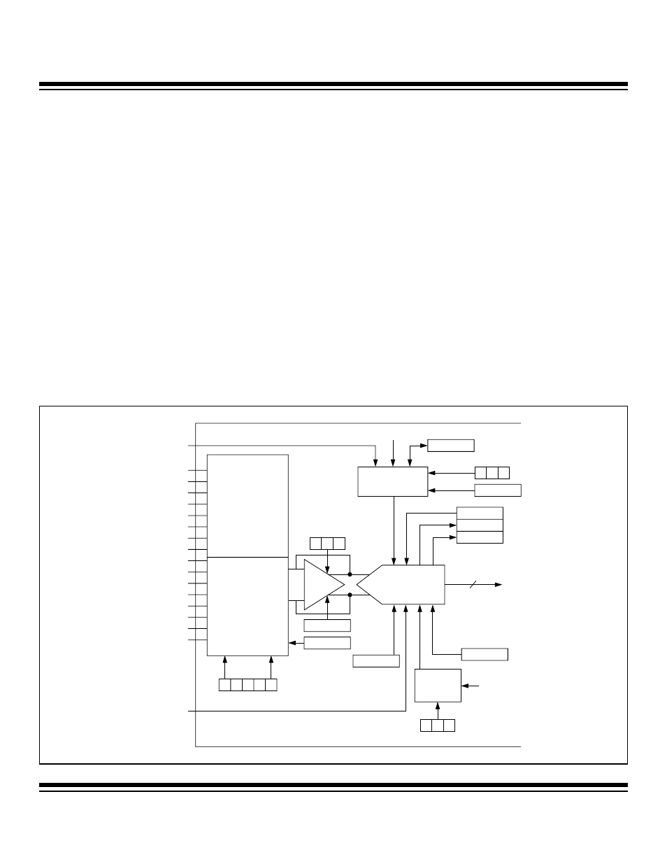
Figure 3-2 shows a simplified functional block diagram of the ADC in differential input configuration.
MAXQ7665/MAXQ7666 User’s Guide
3-17
Figure 3-2. Differential Input ADC Block Diagram
AIN0
AIN2
AIN4
AIN6
AIN8
AIN10
AIN12
AIN14
AIN1
AIN3
AIN5
AIN7
AIN9
AIN11
AIN13
AIN15
PO.4/ADCCNV
CONVERSION
CONTROL
ADCBY
TIMERS 0, 1, 2
ADCDUL
ADCS
2
1
0
2
1
0
PGG
ADCRDY
ADCOV
ADCBIP
PGAE
ADCE
REFADC
ADC
CLOCK
DIV
ADCASD
12
DATA
BUS
0
1
2
3
4
ADCMX
2
1
0
ADCCD
SYSTEM
CLOCK
8:1
MUX
8:1
MUX
12-BIT ADC
500ksps
ADCDIF
PGA
1 TO 32
Maxim Integrated