1 power-supply/supervisory module pins -5, 1 power-supply/supervisory module pins – Maxim Integrated MAXQ7666 User Manual
Page 77
2.1.1 Power-Supply/Supervisory Module Pins
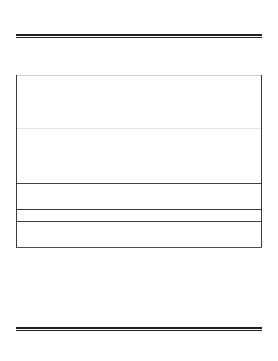
The power-supply module signals are shown in Table 2-1.
Table 2-1. MAXQ7665/MAXQ7666 Power-Supply/Supervisory Module Pins
PIN NUMBER
POWER-SUPPLY
SIGNAL
48 56
FUNCTION
AVDD 44
50
Analog V
DD
Supply. AVDD is the power supply for all analog input/output functions including ADC,
PGA, DAC, and temperature sensor. For the MAXQ7665/MAXQ7666, the analog supply voltage is
+5.0V. If required, connect AVDD to DVDDIO through some supply filtering, which can allow for
voltage monitoring on the AVDD line. If AVDD is a separate supply, no voltage monitoring is applied
and the supply voltage should not deviate more than ±300mV from DVDDIO. Bypass AVDD to AGND
with a 0.1
F capacitor placed as close to the device as possible.
AGND
5, 8
5, 8
Analog Ground*
DVDDIO
26, 39
30, 44
Digital Input/Output Supply Voltage. DVDDIO is the power supply for all digital input/output pins
(except XIN, XOUT, and
RESET). For the MAXQ7665/MAXQ7666, the digital I/O supply voltage is
+5.0V. DVDDIO also powers the internal +3.3V linear regulator (if used). Bypass DVDDIO to GNDIO
with a 0.1
F capacitor placed as close to the device as possible.
GNDIO 27 31
Digital Input/Output Ground. GNDIO is the ground for all the digital I/O pins (except XIN, XOUT,
RESET).*
REGEN
38 43
Active-Low Linear Power Regulator Enable Input.
REGEN controls the internal +3.3V linear regulator.
When
REGEN is connected GNDIO, the linear regulator is enabled; when REGEN is connected to
DVDDIO, the linear regulator is disabled and an external +3.3V supply must be provided to the DVDD
pin.
DVDD 40
45
Digital Supply Voltage. DVDD is the power supply for all core CPU functions, flash, RAM, oscillator,
and digital peripherals. For the MAXQ7665/MAXQ7666, the digital supply voltage is +3.3V and can be
generated by the internal +3.3V linear regulator. Bypass DVDD to DGND with a 4.7
F ±20% capacitor
with maximum ESR of 0.5
. In addition, bypass DVDD with a 0.1F capacitor. Place both bypass
capacitors as close to the device as possible.
DGND
18, 19, 31
20, 21, 36
Digital Ground. These pins serve as the digital ground for the CPU core functions, flash, SRAM, digital
peripherals, and oscillator port.*
RESET
41 47
Active-Low Reset I/O. This is an active-low open-drain signal with an internal pullup resistor to DVDD.
During POR, this pin remains low until DVDD rises above the default power-on reset threshold and a
timeout period expires.
RESET is pulled low by the internal voltage monitoring circuitry if DVDD falls
below the selected brownout reset threshold. This pin can also be pulled low externally by the user or
internally by the watchdog timer. All these events reset the MAXQ7665/MAXQ7666.
MAXQ7665/MAXQ7666 User’s Guide
2-5
* For PCB layout guidelines, refer to Application Note 801 (
www.maxim-ic.com/AN801
) and Application Note 637 (
www.maxim-ic.com/AN637
).
Maxim Integrated