Maxim Integrated MAXQ7666 User Manual
Page 121
MAXQ7665/MAXQ7666 User’s Guide
3-31
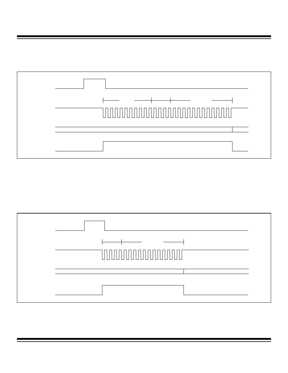
Figure 3-10 shows single-edge-controlled ADC conversion timing when the ADC is in auto shutdown state and the PGA is bypassed.
The power-up and acquisition is triggered by the rising edge of the ADC conversion start source signal ADC_CNVST. ADC_CNVST is
an internal signal generated from a combination of all the three conversion start sources previously described.
In single-edged conversions, the ADC control logic provides the necessary power-up, acquisition, and conversion delay.
a) If ADC is in auto shutdown state, it takes 27 ADC clock cycles before the 12-bit result is available when PGA gain = 1. For PGA
gain > 1, it takes an additional 80 cycles for a total of 107 ADC clock cycles before the 12-bit output result is available.
b) If ADC is not in auto shutdown state, it takes 17 ADC clock cycles before the 12-bit result is available when PGA gain = 1. For
PGA gain > 1, it takes a total of 57 ADC clock cycles before the 12-bit result is available.
Figure 3-11 shows single-edge-controlled ADC conversion when the ADC is not in auto shutdown state and the PGA is bypassed.
Figure 3-10. Single-Edge ADC Conversion Timing; ADC Previously Off and PGA Bypassed
1
17
27
13
ADCBY
ADCDATA
ADCCLK
ADC_CNVST
DATA (n-1)
DATA (n)
ACQUISITION (n)
POWER-UP
CONVERSION (n)
Figure 3-11. Single-Edge ADC Conversion Timing; ADC Previously On and PGA Bypassed
ADCBY
1
17
13
ADCDATA
ADCCLK
ADC_CNVST
DATA (n-1)
DATA (n)
ACQUISITION (n)
CONVERSION (n)
Maxim Integrated