2 in-system programming peripheral registers -3, 1 in-circuit debug flag register (icdf) -3, 2 in-system programming peripheral registers – Maxim Integrated MAXQ7666 User Manual
Page 318: 1 in-circuit debug flag register (icdf)
12.2 In-System Programming Peripheral Registers
The MAXQ7665/MAXQ7666 in-system programming peripheral registers are described here. All the in-system programming peripher-
al registers are directly accessible by the microcontroller through the module/index address.
12.2.1 In-Circuit Debug Flag Register (ICDF)
Register Description:
In-Circuit Debug Flag Register
Register Name:
ICDF
Register Address:
Module 02h, Index 1Bh
Bits 7 to 4: Reserved.
Bits 3 and 2: Programming Source Select Bits 1 and 0 (PSS1:PSS0). These bits are used to select a programming interface dur-
ing in-system programming when SPE is set to logic 1. Otherwise, the logic values of these bits have no meaning. The logical states
of these bits, when read by the CPU, reflect the logical-OR of the PSS bits that are write accessible by the CPU and those in the sys-
tem programming buffer register (SPB) of the TAP module (which are accessible via JTAG). These bits are read/write accessible for
the CPU and are cleared to 0 by a power-on reset or test-logic-reset. CPU writes to the PSS bits result in clearing of the JTAG
PSS1:PSS0 bits. See Table 12-1.
Bit 1: System Program Enable (SPE). This bit controls the behavior of the MAXQ7665/MAXQ7666 following a reset. The SPE bit is
used for in-system programming support, and its logical state, when read by the CPU, always reflects the logical-OR of the SPE bit
that is write accessible by the CPU and the SPE bit of the SPB register in the TAP module, which is accessible via JTAG. The logical
state of this bit determines the program flow after a reset.
0 = The MAXQ7665/MAXQ7666 jump to application code in flash at 0000h following a reset.
1 = The MAXQ7665/MAXQ7666 execute the in-system programming boot loader following a reset.
This bit allows read/write access by the CPU and is cleared to 0 only on a power-on reset or test-logic-reset. The JTAG SPE bit is
cleared by hardware when the ROD bit is set. CPU writes to the SPE bit result in clearing of the JTAG PSS1:PSS0 bits.
Bit 0: Serial Transfer Complete (TXC). See
Section 11 for more information on this bit.
MAXQ7665/MAXQ7666 User’s Guide
12-3
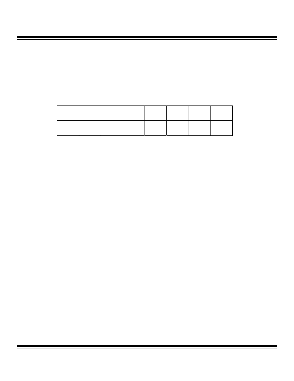
Bit #
7
6
5
4
3
2
1
0
Name
— — — —
PSS1
PSS0
SPE
TXC
Reset
0 0 0 0 0 0 0 0
Access
r r r r rw rw rw rw
r = read, w = write
Maxim Integrated