4 stack memory -15, 5 pseudo-von neumann memory mapping -15 – Maxim Integrated MAXQ7666 User Manual
Page 17
1.2.3.4 Stack Memory
The MAXQ7665/MAXQ7666 provide a 16 x 16 hardware stack to support subroutine calls and system interrupts. A 16-bit wide on-chip
stack is provided by the MAXQ7665/MAXQ7666 for storage of program return addresses and general-purpose use. The stack is used
automatically by the processor when the CALL, RET, and RETI instructions are executed and when an interrupt is serviced; it can also
be used explicitly to store and retrieve data by using the @SP- - source, @++SP destination, or the PUSH, POP, and POPI instructions.
The POPI instruction acts identically to the POP instruction except that it additionally clears the INS bit.
The width of the stack is 16 bits to accommodate the instruction pointer size. The stack depth is 16 for the MAXQ7665/MAXQ7666. As
the stack pointer register SP is used to hold the index of the top of the stack, the maximum size of the stack allowed is defined by the
number of bits defined in the SP register (e.g., 4 bits for stack depth of 16).
On reset, the stack pointer SP initializes to the top of the stack (e.g. 0Fh for a 16-word stack). The CALL, PUSH, and interrupt vector-
ing operations increment SP and then store a value at @SP. The RET, RETI, POP, and POPI operations retrieve the value at @SP and
then decrement SP.
As with the other RAM-based modules, the stack memory is initialized to indeterminate values upon reset or power-up. Stack memory
is dedicated for stack operations only and cannot be accessed through program or data address spaces.
When using the in-circuit debugging features of the MAXQ7665/MAXQ7666, one word of the stack must be reserved to store the return
location when execution branches into the debugging routines in the utility ROM. If in-circuit debug will not be used, the entire stack
is available for application use.
1.2.3.5 Pseudo-Von Neumann Memory Mapping
The MAXQ7665/MAXQ7666 support a pseudo-Von Neumann memory structure that can merge program and data into a linear mem-
ory map. This is accomplished by mapping the data memory into the program space or mapping program memory segment into the
data space. Program memory from 0000h to 7FFFh is the normal user code segment, followed by the utility ROM segment. The upper-
most part of the 64kWord memory is the logical area for data memory when accessed as a code segment.
The program memory is logically divided into four program pages:
• P0 contains the lower 16kWords,
• P1 contains the second 16kWords,
• P2 contains the third 16kWords, and
• P3 contains the fourth 16kWords.
By default, P2 and P3 are not accessible for program execution until they are explicitly activated by the user software. The Upper
Program Access (UPA) bit must be set to logic 1 to activate P2 and P3. Once UPA is set, P2 and P3 will occupy the upper half of the
64kWord program space. In this configuration (UPA = 1), the utility ROM cannot be accessed as program memory and the physical
data memory cannot be accessed logically in program space.
The logical mapping of physical program memory page(s) into data space depends upon two factors: physical memory currently in
use for program execution; and word/byte data memory access selection. If execution is from the utility ROM, physical program mem-
ory page(s) can logically be mapped to the upper half of data memory space. If logical data memory is used for execution, physical
program memory page(s) can logically be mapped to the lower half of data memory space. If byte access mode is selected, only one
page (16kWords) may be logically mapped, as just defined, to either the upper or lower half of data memory. If word access mode is
selected, two pages (32kWords total) may be logically mapped to data memory. To avoid memory overlapping in the byte access
mode, the physical data memory should be confined to the address range 0000h to 3FFFh in word mode. The selection of physical
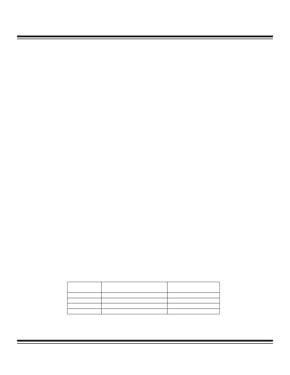
memory page or pages to be logically mapped to data space is determined by the Code Access Bits (CDA1:0):
Figure 1-4 summarizes the default memory maps for this memory structure. The primary difference lies in the reset default settings for
the data pointer Word/Byte Mode Select (WBSn) bits. The WBSn bits of the MAXQ7665/MAXQ7666 default to word access mode
(WBSn = 1).
MAXQ7665/MAXQ7666 User’s Guide
1-15
CDA1:0
SELECTED PAGE IN BYTE MODE
SELECTED PAGE IN
WORD MODE
00
P0
P0 and P1
01
P1
P0 and P1
10
P2
P2 and P3
11
P3
P2 and P3
Maxim Integrated