4 system register descriptions -43, 4 system register descriptions – Maxim Integrated MAXQ7666 User Manual
Page 45
move @BP[--Offs], @BP[Offs++]
move @DP[0], @DP[0]++
move @DP[1], @DP[1]++
move @BP[Offs], @BP[Offs++]
move @DP[0], @DP[0]--
move @DP[1], @DP[1]--
move @BP[Offs], @BP[Offs--]
move DP[0], @DP[0]++
move DP[0], @DP[0]--
move DP[1], @DP[1]++
move DP[1], @DP[1]--
move Offs, @BP[Offs--]
move Offs, @BP[Offs++]
1.4 System Register Descriptions
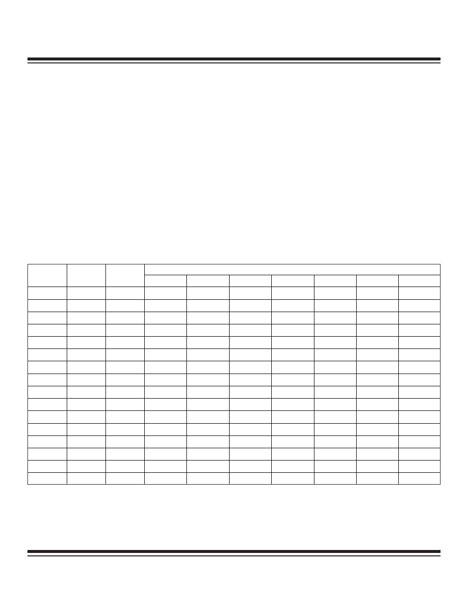
The MAXQ7665/MAXQ7666 system register map is shown in Table 1-8. The system register bit functions and reset value are shown in
Table 1-9. Those registers defined in the MAXQ7665/MAXQ7666 system register map are described in the following sections. The
address for each register are given in the format
module[index], where module is the module specifier from 8h to Fh and index is the
register subindex from 0h to Fh.
Table 1-8. MAXQ7665/MAXQ7666 System Register Map
MAXQ7665/MAXQ7666 User’s Guide
1-43
MODULE NAME (BASE SPECIFIER)
CYCLES TO
READ
CYCLES TO
WRITE
REGISTER
INDEX
AP (8h)
A (9h)
PFX (Bh)
IP (Ch)
SP (Dh)
DPC (Eh)
DP (Fh)
1 1 0h AP
A[0]
PFX[0]
IP
1 1 1h
APC
A[1]
PFX[1]
SP
1 1 2h A[2]
PFX[2]
IV
1 1 3h A[3]
PFX[3]
OFFS
DP0
1 1 4h
PSF
A[4]
PFX[4]
DPC
1 1 5h IC A[5]
PFX[5]
GR
1 1 6h
IMR
A[6]
PFX[6]
LC0
GRL
1 1 7h A[7]
PFX[7]
LC1
BP
DP1
1 2 8h SC
A[8]
GRS
1 2 9h A[9]
GRH
1 2 Ah A[10]
GRXL
1 2 Bh IIR
A[11]
FP
1 2 Ch A[12]
1 2 Dh A[13]
1 2 Eh
CKCN
A[14]
1 2 Fh
WDCN
A[15]
Note: Names that appear in italics indicate that all bits of a register are read-only. Names that appear in bold indicate that a register is 16 bits wide.
Maxim Integrated