2 oscillator control register (oscc) -6, 2 oscillator control register (oscc) – Maxim Integrated MAXQ7666 User Manual
Page 203
5.2.2 Oscillator Control Register (OSCC)
The OSCC register contains the oscillator enable and configuration bits.
Register Description:
Oscillator Control Register
Register Name:
OSCC
Register Address:
Module 05h, Index 0Ch
Bits 15 to 12, 4, and 3: Reserved. Read 0, write ignored.
Bits 11 and 10: High-Frequency Crystal Output Capacitance Select 1 and 0 (HFOC1 and HFOC0). These bits select the output
capacitance of the on-chip high-frequency oscillator. The capacitor value is switched on to the XOUT pin of the MAXQ7665. The pos-
sible selections are given below. Note: For the default 00 setting, only a 1.3pF capacitor is switched on. The 6pF capacitor value is
essentially due to stray capacitance.
Note: For the MAXQ7666, the HFIC1:HFIC0 bits select both the input and output capacitance of the on-chip high-frequency oscillator.
The HFOC1:HFOC0 bits are used to select one of four possible crystal drive strengths as shown in the following table. Refer to the
MAXQ7666 data sheet for typical drive strengths.
MAXQ7665/MAXQ7666 User’s Guide
5-6
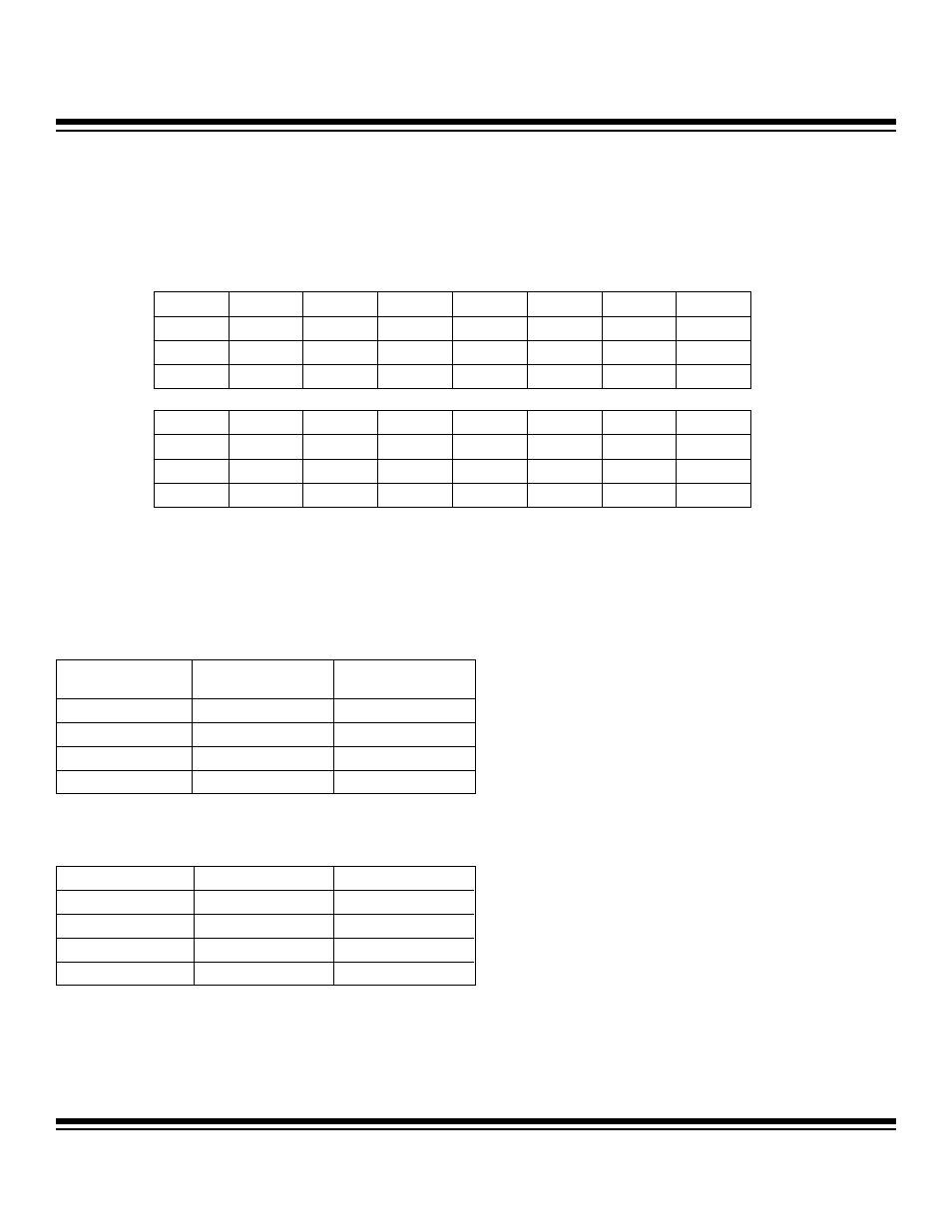
Bit #
15
14
13
12
11
10
9
8
Name — — — —
HFOC1
HFOC0
HFIC1
HFIC0
Reset 0 0 0 0 0 0 0 0
Access r r
r
r
rw
rw
rw
rw
Bit #
7
6
5
4
3
2
1
0
Name
ADCD2 ADCD1 ADCD0
—
—
EXTHF RCE
HFE
Reset 0 0 0 0 0 0 1 0
Access rw rw
rw
r
r
rw
rw
rw
r = read, w = write
Note: This register is cleared to 0002h on power-on reset and is not affected by other forms of reset.
HFOC1 HFOC0
CAPACITOR VALUE
(pF)
0 0
6
(default)
0 1 17
1 0 27
1 1 34
HFOC1
HFOC0
DRIVE STRENGTH
0 0
Drive
2
(default)
0 1
Drive
3
(highest)
1 0
Drive
0
(smallest)
1 1
Drive
1
Maxim Integrated