Measurement Computing DBK Part 2 User Manual
Page 29
DBK Option Cards and Module
899892
DBK43A & DBK43B, pg. 9
Input Configuration Headers
Eight 2×6 pin-headers with pin numbers 1 to 12 are on the board, 1 for each channel designated H100 (channel 0) to
H800 (channel 7). The user can position jumpers on this header to configure inputs from a variety of bridge types.
Jumping header pins 1-to-2 and 3-to-4 connects the +Vin and -Vin to the calibration MUX for different
bridge configurations.
Jumping pins 5-to-7 and 9-to-11 allows internal sense regulation of the excitation regulator.
Jumping pins 5-to-6 and 11-to-12 allows for remote excitation sensing.
Jumping pin 10-to-12 allows the use of a remote shunt-calibration resistor.
See previous figure for header configurations that correspond with different bridge-wiring schemes.
Resistor Sockets and Adapter Plugs
Eight 2×8 resistor sockets with rows numbered A to H are on the board; 1 socket for each channel and designated
R100 (channel 0) to R800 (channel 7). An adapter plug for soldering resistors is included for each channel; user-
soldered plugs facilitate changing configurations as needed.
Bridge-completion resistors include: Rn00B, Rn00C, Rn00E, and Rn00F. Resistors Rn00A and Rn00G are
used to complete 3-wire strain-gage configurations.
Rn00D and Rn00H are internal shunt resistors from +V in and -V in respectively to -excitation.
Match the proper row as shown in the figure, Bridge-Configuration Settings
for DBK43A and DBK43B (previous page).
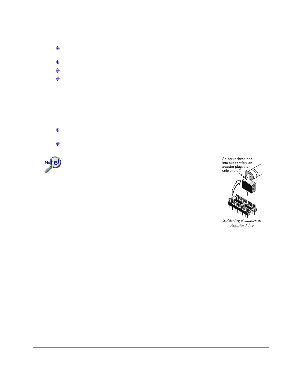
DO NOT just insert resistors into sockets. Such connections are unreliable.
To achieve a reliable connection, solder resistors to the adapter plug
Soldering should be done with the plug inserted into the resistor socket;
otherwise, heat from soldering can distort the shape of the plug.
After soldering, the resistor leads should be snipped off close to the support
to prevent contact with other components.
Handle the adaptor plugs with care to prevent pin damage.
Shunt-Calibration Resistors
DBK43A and DBK43B provide physical locations for internal shunt-calibration resistors. Each channel has resistor
locations that can be shunted across one or the other of the lower bridge arms by a hardware and software-accessible
solid state switch (FET transistor) to create a repeatable bridge imbalance with a precision resistor.
For any balanced bridge, a resistance value can be applied in parallel with one of the four bridge elements to create
a predictable imbalance and output voltage. For example, a 350
Ω 2mV/V strain gage will deliver full output if one
arm drops by 0.8% (about 2.80
Ω) to 347.2Ω. A 43.4 KΩ resistance shunted across one or the other lower bridge
elements will result in full-positive (Rn00H) or full-negative (Rn00D) output. For best results, Rn00H and Rn00D
should be across the strain element when it is switched in.