Input signal conditioning, Warning – Measurement Computing DBK Part 2 User Manual
Page 113
Input Signal Conditioning
The DBK55 conditions the input signal in several ways to provide the best output accuracy. Reducing
noise and limiting the bandwidth are the first steps in the conditioning process and are done in hardware.
Software can further clean up the signal by selecting the cleanest edge to read and by setting a debounce
delay to ignore spurious signals. The debounce concept is discussed on page 4.
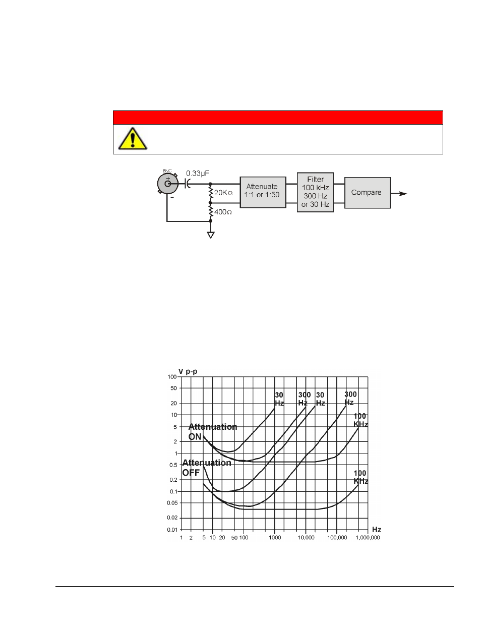
Analog Input Signal Conditioning
WARNING
Input voltages should be at least 50 mV peak-to-peak. The maximum analog input
signal is 30 Vrms (42 Vpeak, 84 Vp-p). Stronger signals may damage the DBK55 or
present an electrical shock hazard.
When a channel’s two “input circuit jumpers” are set for analog, the center conductor of the BNC
connector is AC-coupled through a 0.33 µF capacitor to the attenuator. The outside conductor connects to
ground. With the attenuator disabled [full sensitivity] input-protection diodes limit the signal to about 1.5
Vp-p. Larger signals will see an impedance of 6.7 K
Ω (rather than 20 KΩ) in series with 0.33 µF. With
the attenuator enabled, the input impedance remains 20 K
Ω regardless of the input level.
After AC-coupling, attenuation and filtering, a comparator converts the input signal into a clean digital
signal. The comparator output is high when the center-pin signal is higher than the outside-conductor
signal and low when the center-pin is lower than the outside-conductor signal. The comparator has
hysteresis to reduce the effects of noise by ignoring small signals.
The following graph shows typical sine-wave sensitivity in peak-to-peak voltage vs frequency. Six
combinations of attenuation (on/off) and low-pass filtering (30 Hz, 300 Hz, and 100 kHz) are graphed.
Digital Input Signal Conditioning
DBK Option Cards and Modules
988793
DBK55, pg. 3