External power watchdog, Operation – Measurement Computing DBK Part 2 User Manual
Page 241
External Power Watchdog
The External Power Watchdog is governed by the setting of the JP2 jumper. This jumper allows the user
to determine the behavior of the digital output latches in the event of a loss and recovery of the external
power supply.
With the jumper in the ENABLE position, the loss of external power will cause the output latches to be
reset into a high-impedance condition. Even with a recovery of the external power, all output modules will
be disabled until a write is done to the data bus. This setting is useful in an application that requires a
serial enabling of output loads.
With the jumper in the DISABLE position, the loss of external power will have no effect on the state or
continued control of the output latches. That is, data that is written to the output modules will continue to
be latches as normal. A recovery of the external power would then cause the output modules to reflect the
current state of the output latches. This setting is useful in the case where the operator halts the transfer of
data and turns off the external power on purpose and then wants the system to assume the same state upon
recovery of the external power.
The setting of the JP2 jumper has no effect on input modules with regards to external power. While a loss
of external power will result in corruption of the data being read, the data bus will be valid again
immediately upon the recovery of the external power. The default setting of the JP2 jumper is the
ENABLE position.
Operation
The DBK208 P2 expansion protocol makes use of a 4-bit dip switch (S1) to configure the board’s
addresses. Addresses are seen as XXXX + 0 for Bank 0’s set of eight modules and as XXXX + 1 for Bank
1’s set of eight modules, where the four Xs represent the DIP switch settings of 16 8 4 and 2. With all
four S1 micro-switches OFF (open), the first system board (designate as “0”) has Bank 0 registered as 0
and Bank 1 registered as 1. With S1’s micro-switch “2” closed, we would see Bank 0 registered as 2 and
Bank 1 registered as 3. The following table portrays the addressing scheme and includes DaqView
designations.
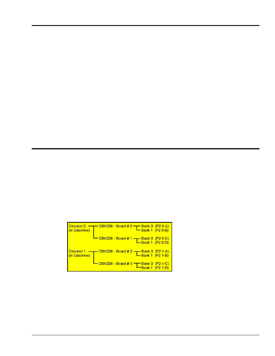
The following breakdown is provided to indicate the relationship of DaqView channels to DBK208 boards
and banks. More detailed information follows.
Simplified Channel-to-DBK208 Relationship
DBK Option Cards and Modules
987594
DBK208, pg. 5