Caution, Edge selection, Debouncing – Measurement Computing DBK Part 2 User Manual
Page 114

CAUTION
The input signal may range from -15 to +15 V. Higher voltages may damage the
DBK55.
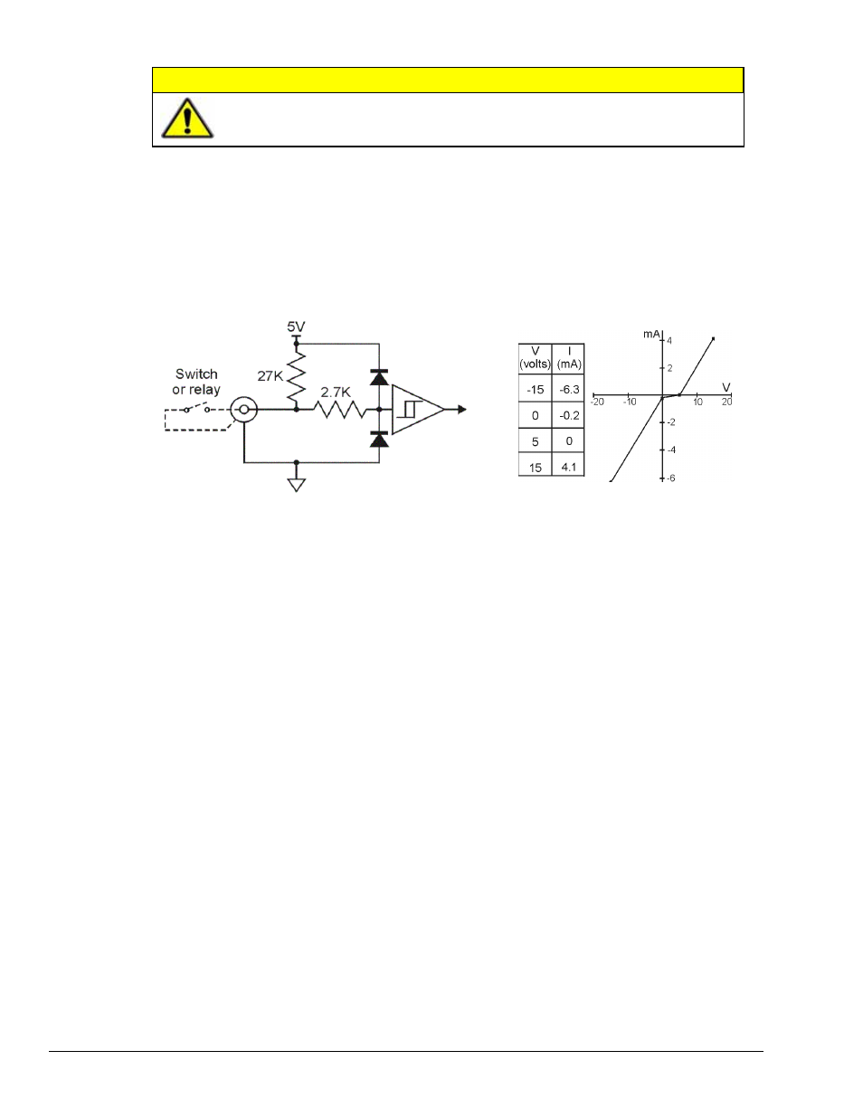
The digital input circuit is represented in the left-hand figure, below. When both of a channel’s “input
circuit jumpers” are set for digital, the outside (shield) conductor of the BNC connector connects to
ground. The center conductor is pulled up with 27 K
Ω to +5 V and then passes through a 2.7 KΩ
protection resistor before being detected by a Schmitt-trigger buffer with input-protection diodes.
The input thresholds are fixed TTL levels. Below 0.5 V (0.8 V typical), the Schmitt-trigger buffer output
is low. Above 2.1 V (1.6 V typical), the buffer output is high. The 27 K
Ω pull-up resistor allows the
digital inputs to sense switches or relays connected directly to the DBK55 as shown in the figure. The
debounce circuit can remove noise effects of switching. Debouncing is discussed later on this page.
DBK55, pg. 4
988793
DBK Option Cards and Modules
The input impedance for digital signals depends on the signal level. For signals between 0 and 5 V, the
input-protection diodes do not conduct, and the digital input impedance is just the 27 K
Ω pull-up
resistance. For signals less than 0 V or greater than 5 V, the input-protection diodes conduct and the
impedance drops to about 2.4 K
Ω. The figure (upper right) shows the approximate digital-input
current/voltage relationship.
Edge Selection
The DBK55 determines the frequency by measuring the time between successive rising or falling edges of
the input signal. Which edge is electrically cleaner depends on the application and related components. If
rising edges are used, the edge-selection circuit does not modify the signal. If falling edges are used, the
circuit inverts the signal so falling edges appear as rising edges to the subsequent circuits. Through
software, each channel can be independently set for rising- or falling-edge.
Debouncing
Debouncing is a process of ignoring signals too short to be real events. When a relay or switch closes, the
electrical contacts may not initially make good contact. Mechanical vibrations can occur, and contact is
made and broken several times before stabilizing. Counting all these signals would yield too high a
frequency. The debounce circuit solves this problem by ignoring rising edges not preceded by a sustained
low signal. The sustain interval can be set in software to 0, 0.6, 2.5, or 10 ms for each channel.
Debouncing may be disabled (0 ms) for clean, high-frequency signals. Long debounce times will limit
high-frequency response (e.g., a 10 ms debounce will limit the frequency to about 100 Hz). In general, use
“0” (debounce disabled) for clean, high-frequency signals; increase the debounce as needed for noisy, low-
frequency signals from switches and relays.
